
Surfaces that are covered in particular nano-scale patterns have been shown to affect what type of tissue stem cells become when grown in a lab, without the need for hormones or other chemicals to direct the process.
A team of scientists from Manchester University is now planning to work with a manufacturer to develop and test a machine that can economically mass-produce these nano-patterned surfaces, which could also be used in the development of organic electronics.
‘What we want to do is to be able to grow cells in large numbers and then be able to use that essentially for a therapeutic purpose,’ project leader Dr Lu Shin Wong told The Engineer.
‘If you can control the behaviour of stem cells without having to add any of these chemical compounds, that would be very useful because you can then use this to effect behaviour through implanting devices [in a patient] rather than administering drugs.’
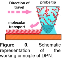
The technique for creating the nano-surfaces, known as dip pen nanolithography (DPN), involves using tiny spikes to deposit a coating on a substrate — like writing with a fountain pen dipped in ink — in order to build up the intricate pattern.
It was originally developed by Prof Chad Mirkin of Northwestern University in Chicago using a modified atomic force microscope (AFM), a device that creates images of a surface by feeling it with a nano-scale probe.
Wong, who previously worked with Mirkin at Northwestern, now wants to explore how DPN could be used in areas such as manufacturing surfaces for use in growing stem cells or creating organic electronic devices utilising polymers that would be damaged by traditional semiconductor manufacturing techniques.
To do this, he plans to work with an AFM manufacturer to develop a device with thousands or even millions of probes that move simultaneously and so can produce a much larger area of nano-surface material.
In order to make sure all the probes come into contact with the surface and produce the same pattern, they must be aligned with a very high degree of accuracy, with a tilt of no more than 0.005º.
‘Alignment is very tedious if you have to do this manually,’ said Wong. ‘What we are in negotiations with the companies to do is see if they can automate that process.
‘You need some kind of software algorithm that will allow it to determine which side was pressed down and then compensate by tilting it the other way.’


Swiss geoengineering start-up targets methane removal
No mention whatsoever about the effect of increased methane levels/iron chloride in the ocean on the pH and chemical properties of the ocean - are we...