The study from the University of Pennsylvania, which is published in Science, reportedly opens the door for electrical components to be built into flexible or wearable applications, as the lower-temperature process is said to be compatible with an array of materials and can be applied to larger areas.
The researchers' nanocrystal-based field effect transistors were patterned onto flexible plastic backings using spin coating but could eventually be constructed by additive manufacturing systems.
The study was lead by Cherie Kagan, the Stephen J. Angello Professor in the School of Engineering and Applied Science, and Ji-Hyuk Choi, formerly a member of her lab and now a senior researcher at the Korea Institute of Geoscience and Mineral Resources.
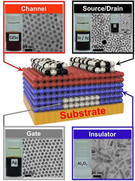
The researchers began by taking nanocrystals, or roughly spherical nanoscale particles, with the electrical qualities necessary for a transistor and dispersing these particles in a liquid, making nanocrystal inks.
Kagan's group developed a library of four of these inks: a conductor (silver), an insulator (aluminium oxide), a semiconductor (cadmium selenide) and a conductor combined with a dopant (a mixture of silver and indium).
"These materials are colloids just like the ink in your inkjet printer but you can get all the characteristics that you want and expect from the analogous bulk materials, such as whether they're conductors, semiconductors or insulators,” Kagan said in a statement. "Our question was whether you could lay them down on a surface in such a way that they work together to form functional transistors."
The electrical properties of several of these nanocrystal inks had been independently verified, but they had never been combined into full devices.
"This is the first work showing that all the components, the metallic, insulating, and semiconducting layers of the transistors, and even the doping of the semiconductor could be made from nanocrystals,” Choi said,
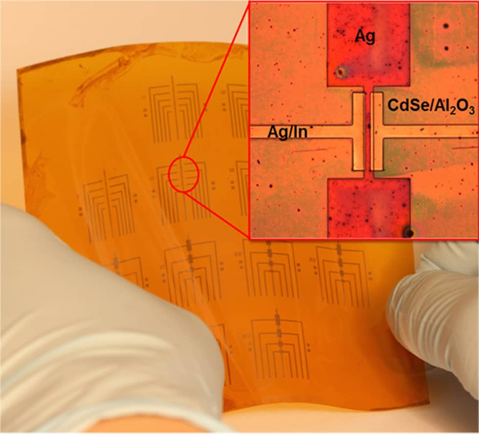
The process requires layering or mixing them in precise patterns. First, the conductive silver nanocrystal ink was deposited from liquid on a flexible plastic surface that was treated with a photolithographic mask, and then rapidly spun to draw it out in an even layer. The mask was then removed to leave the silver ink in the shape of the transistor's gate electrode.
The researchers followed that layer by spin-coating a layer of the aluminium oxide nanocrystal-based insulator, then a layer of the cadmium selenide nanocrystal-based semiconductor and finally another masked layer for the indium/silver mixture, which forms the transistor's source and drain electrodes. On heating at relatively low temperatures, the indium dopant diffused from those electrodes into the semiconductor component.
"The trick with working with solution-based materials is making sure that, when you add the second layer, it doesn't wash off the first, and so on," Kagan said. "We had to treat the surfaces of the nanocrystals, both when they're first in solution and after they're deposited, to make sure they have the right electrical properties and that they stick together in the configuration we want."
Because this entirely ink-based fabrication process works at lower temperatures than existing vacuum-based methods, the researchers were able to make several transistors on the same flexible plastic backing at the same time.


Red Bull makes hydrogen fuel cell play with AVL
Formula 1 is an anachronistic anomaly where its only cutting edge is in engine development. The rules prohibit any real innovation and there would be...