The team, comprised of scientists and engineers from Northwestern University, the University of Illinois and Tsinghua University, published work earlier in the year on a ‘pop-up’ fabrication technique it had developed. Using kirigami, the Japanese art of folding and cutting, the team has been able to build on this work by creating more useful structures.
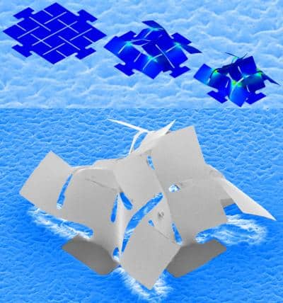
“The key concept in kirigami is a cut,” said Yonggang Huang, a professor at Northwestern’s McCormick School of Engineering.
“Cuts usually lead to failure, but here we have the opposite: cuts allow us to produce complex 3D shapes we wouldn’t have otherwise. This unique 3D fabrication technique now can be used by others for their own creations and applications.”
The study is published in the Proceedings of the National Academy of Sciences. It shows how the team made 3D structures from materials including silicon, polymers, metals and dielectrics. Some structures combined a number of materials, such as gold and a semiconductor, including patterns that provide useful optical responses.
Due to the wide range of materials available, and the speed with which kirigami structures can be assembled, the team believes the new technique has a range of advantages that make it a viable alternative to 3D printing.
“Our approach offers remarkable flexibility in transforming 2D structures, including those found in the most advanced forms of electronics and photonics, into 3D structures,” said John A. Rogers, professor of materials science and engineering at the University of Illinois.
“We have successfully established a set of design rules and methods for manipulating sheets, ribbons and plates and controlling their behaviour in 3D space.”
According to Huang, the cuts are not actually made physically, but are instead engineered into the material with the precise methods of manufacturing used in computer chip production. The size of the resulting 3D structures is extremely small, ranging from 100 nanometres square to 3 centimetres square. The cuts themselves are smaller again, typically between 1 micron and 10 microns wide for silicon 3D structures.


Red Bull makes hydrogen fuel cell play with AVL
Formula 1 is an anachronistic anomaly where its only cutting edge is in engine development. The rules prohibit any real innovation and there would be...