The research, from the University of Minnesota, Argonne National Laboratory and Seoul National University, is published in Nature Communications.
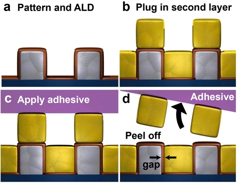
Combining several standard nanofabrication techniques - and low-tech adhesive tape - researchers at the University of Minnesota created extremely thin gaps through a layer of metal and patterned these gaps over the entire surface of a four-inch silicon wafer.
According to the University of Minnesota, the smallest gaps were one nanometre wide, which is said to be much smaller than most researchers have been able to achieve. In addition, the widths of the gaps could be controlled on the atomic level, thereby providing the basis for producing new and better nanostructures that are at the core of advanced electronic and optical devices.
One of the potential uses of nanometre-scale gaps in metal layers is to shine light into spaces much smaller than is otherwise possible. Collaborators at Seoul National University, led by Prof Dai-Sik Kim, and Argonne National Laboratory, led by Dr. Matthew Pelton, showed that light could readily be shone through these gaps, even though the gaps are hundreds or even thousands of times smaller than the wavelength of the light used.
Researchers are very interested in forcing light into small spaces because this is a way of boosting the intensity of the light. The collaborators found that the intensity inside the gaps is increased by as much as 600 million times.
‘Our technology, called atomic layer lithography, has the potential to create ultra-small sensors with increased sensitivity and also enable new and exciting experiments at the nanoscale like we’ve never been able to do before,’ said Sang-Hyun Oh, one of the lead researchers on the study and a professor of electrical and computer engineering in the University of Minnesota’s College of Science and Engineering. ‘This research also provides the basis for future studies to improve electronic and photonic devices.’
Sticky solution
One of the most surprising outcomes of the research is that adhesive tape was one of the keys to the discovery as etching one-nanometre-wide gaps into metals is not feasible with existing tools.
Instead, the researchers in Oh’s team constructed the nanogaps by layering atomic-scale thin films on the sides of metal patterns and then capping the structure with another metal layer. No expensive patterning tools were needed to form the gaps this way, but it was challenging to remove the excess metals on top and expose the tiny gaps.
Whilst trying to work out how to remove the metal films, University of Minnesota Ph.D. student and lead author of the study Xiaoshu Chen found that adhesive tape could remove the excess metals.
‘The Scotch tape works nicely, which was unexpected,’ Oh said in a statement. ‘Our technique is so simple yet can create uniform and ultra-small gaps like we’ve never been able to do before. We hope that it will rapidly be taken up by many researchers.’
Their research paper - Atomic layer lithography of wafer-scale nanogap arrays for extreme confinement of electromagnetic waves - can be found here.


April 1886: the Brunkebergs tunnel
First ever example of a ground source heat pump?