
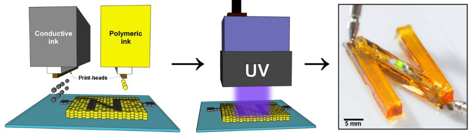
The circuits contain electrically-conductive metallic inks and insulating polymeric inks that are produced in a single inkjet printing process where UV light solidifies the inks.
According to the university, the technique paves the way for the electronics manufacturers to produce fully functional components such as 3D antennae and sensors from multiple materials including metals and plastics.
The new method is said to combine 2D printed electronics with 3D printing to create 3D products. This expands the impact of Multifunctional Additive Manufacturing (MFAM), which involves printing multiple materials in a single additive manufacturing system to create components with broader functionalities.
The new method is claimed to overcome some of the challenges in manufacturing fully functional devices that contain plastic and metal components in complex structures, where different methods are required to solidify each material.
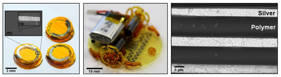
Existing systems typically use one material which limits the functionality of the printed structures. Having two materials like a conductor and an insulator expands the range of functions in electronics. A wristband which includes a pressure sensor and wireless communication circuitry could be 3D printed and customised for the wearer in a single process.
The breakthrough speeds up the solidification process of the conductive inks to less than a minute per layer. Previously, this process took much longer to be completed using ovens and hot plates, making it impractical when hundreds of layers are needed to form an object. In addition, the production of electronic circuits and devices is limited by current manufacturing methods that restrict the form, and potentially the performance, of these systems.
Prof Chris Tuck, Professor of Materials Engineering and lead investigator of the study, said: “Being able to 3D print conductive and dielectric materials in a single structure with the high precision that inkjet printing offers, will enable the fabrication of fully customised electronic components. You don’t have to select standard values for capacitors when you design a circuit, you just set the value and the printer will produce the component for you."
Dr Ehab Saleh and members of the team from CfAM found that silver nanoparticles in conductive inks are capable of absorbing UV light efficiently. The absorbed UV energy is converted into heat, which evaporates solvents of the conductive ink and fuses the silver nanoparticles. This process affects only the conductive ink and does not damage any adjacent printed polymers. The researchers used the same LED-based UV light to convert polymeric inks into solids in the same printing process to form multi-material 3D structures.
The project has so far led to collaborations to develop medical devices, radio frequency shielding surfaces and novel structures for harvesting solar energy.


Nanogenerator consumes CO2 to generate electricity
Whoopee, they've solved how to keep a light on but not a lot else.