
Scientists from Russia, Singapore and the US have used AI to predict changes to material properties under strain, which could lead to the engineering of new tailored materials.
Strain engineering has wide implications for technology in general. It has previously been demonstrated that it has the potential to improve the performance of silicon chips by as much as 50 per cent, as well as manipulate nanoneedles made from diamond.
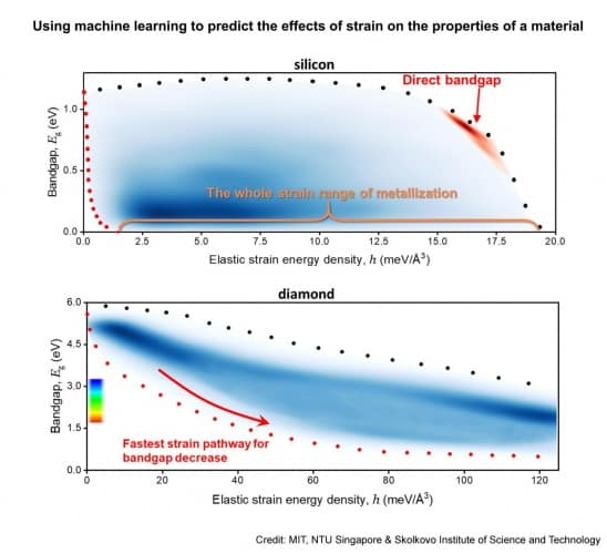
In the new study, published in in the Proceedings of the National Academy of Sciences, the researchers describe how machine learning was used to identify the most energy-efficient strain pathways that could transform diamond into more effective semiconductors. Strain can be applied in any of six different and independent ways (in three different dimensions, each one of which can produce strain in-and-out or sideways), and with nearly infinite gradations of degree, so the number of possibilities is impractical to explore simply by trial and error.
"It quickly grows to 100 million calculations if we want to map out the entire elastic strain space," said Ju Li, Professor of Nuclear Science and Engineering and Materials Science and Engineering at MIT.
Rather than guesswork, the new method used AI to predict the effects of strain on the properties of a material. According to Professor Subra Suresh, President of NTU Singapore and senior study author, this makes it possible to more efficiently explore the virtually infinite possible combinations of material strain in a six-dimensional strain space.
"Now we have this reasonably accurate method that drastically reduces the complexity of the calculations needed," said Prof Suresh, who is also a former Dean of Engineering at MIT.
"Our research is an illustration of how recent advances in seemingly distant fields such as material physics, artificial intelligence, computing, and machine learning can be brought together to advance scientific knowledge that has strong implications for industry application."
The team claims the work opens up new materials possibilities for electronic, optoelectronic, and photonic devices that could find uses for communications, information processing, and energy applications.


Swiss geoengineering start-up targets methane removal
No mention whatsoever about the effect of increased methane levels/iron chloride in the ocean on the pH and chemical properties of the ocean - are we...