
This article highlights the advances in microwave circuit design in recent years, which now mean that low phase noise VCOs on silicon technology can cover an octave range of frequency. Integrated output dividers on the same IC permit several octaves of lower frequency coverage, and multipliers allow frequencies as great as 32 GHz to be generated using a single IC. Advances in fractional-N PLL synthesizers now mean that overall rms jitter at microwave frequencies can be as low as 60 fs, with infinitesimal frequency resolution and minimal spurious tones. Low insertion loss wideband filters can be used with these integrated PLL/VCO ICs to improve the spectral performance of the entire system, greatly simplifying the challenge of microwave and millimeter wave local oscillator generation.
Introduction
Local oscillators (LOs) are a vital component in modern communication, automotive, industrial, and instrumentation applications. Whether up- or downconverting frequencies from baseband to RF and vice versa, generating ramp frequencies for automotive radar applications, material sensing, or developing the instrumentation to build and test the circuits for these applications, LOs are present in many aspects of our lives. Advances in circuit and process technology have helped reduce the cost, complexity, and area of such circuits, and design-in efforts for LOs are greatly simplified with modern integrated circuits compared to the past, which required a more diverse mix of active and passive technologies.
In the past, the majority of LOs for 2G communications applications like GSM, used integer-N PLLs similar to Analog Devices’ ADF4106, together with a narrow-band T-package VCO (example VCO190-1846T). For the most part, the high quality factor (Q) of these VCOs made them very suitable for meeting the demanding phase noise specifications of this standard. Cellphones of that time generally supported only one wireless standard, and the standard itself had limited data rates (although excellent coverage enabled by 2G networks helped cellular phones win broad market acceptance). Base-station LOs tended to be modules assembled using various ICs and VCO submodules, as seen in Figure 1.
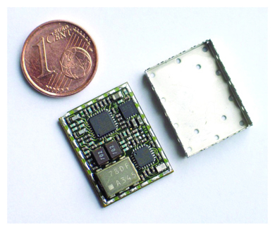
Figure 1. LO module for wireless communications.
Greater demand for over-the-air data rates and compatibility with different global wireless standards drove the development of wideband VCOs, which would facilitate wider frequency coverage and support increasing amounts of the newly available frequency spectrum than was feasible using a narrow-band VCO. The microwave backhaul network supporting this data throughput also came under pressure to support higher order modulation rates, and to be more configurable for different ranges and standards, to enable network providers to reduce engineering effort and improve return on investment. Supporting the development of these networks, a typical signal analyzer used large and heavy yttrium iron garnet (YIG) oscillators and filtering that employed similarly bulky technology.
VCO Improvements
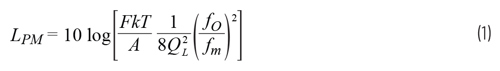
The most significant technical challenge to the development of integrated silicon microwave VCOs was the limited Q possible on available wafer fabrication processes. In many cases, the Q would fall from 100s typical of wire-wound inductors (used in T-package VCOs), to just over 10, severely impacting phase noise due to the constraints imposed by Leeson’s equation, in which phase noise LPM (Equation 1) has an inverse square relationship with higher VCO Q and, by extension, lower frequency range.
Wideband single-core VCOs fabricated on gallium arsenide (GaAs) or silicon germanium (SiGe), solved the problem of range vs. noise by extending the tuning port range of the VCO from 5 V (typically that available from most silicon-based PLL charge pumps) to 15 V or even 30 V. This meant that the resonator Q could remain the same, but that the extended varactor tunability offered a wider tuning range without a degradation in phase noise. This higher tuning range posed a challenge solved by using active low-pass filters, translating the charge pump voltage (typically 5 V) to 15 V or 30 V (see tuning range of the HMC733 in Figure 2). These active filters require high voltage, low noise op amps. A typical microwave LO would thus consist of the PLL (ADF4106) together with an op amp, GaAs VCO, and, in many cases, an additional external divider to divide the VCO signal to the maximum permitted input frequency of the PLL (6 GHz in the case of the ADF4106). GaAs VCOs typically operated in the S-band and higher, as the resonator circuits generally give best performance above 2 GHz. Great care and attention was required in designing the circuit board, which required a high degree of expertise in power supply, analog, and the RF and microwave domains. Designing the PLL filter and simulating its performance required a lot of experience with control theory and noise modeling, and familiarity with each individual component. The experience required to achieve this set of tasks wasn’t easily acquired and tended to reside with senior individuals with decades of experience in hardware design.
A number of technologies exist that address the low Q. On a part family like the ADF4360, bond wires across the top of the die (attached to bond pads) provide a Q factor of ~30. Thick metal inductors also improved Q, and improvements to varactor Q greatly helped increase resonator Q and led to further phase noise improvements. The BiCMOS processes used for the high frequency VCO and N divider circuitry, together with various CMOS logic circuits for switching in and out the various capacitors meant that wideband PLL and VCO ICs were feasible, and their smaller size and wider frequency range led to their rapid adoption in the wireless market.
This approach was followed for many wideband LOs. A VCO covering a full octave range is highly advantageous, as a bank of frequency dividers allows the generation of frequencies limited only by the lowest available VCO frequency, and the highest available divider ratio. A significant breakthrough in VCO design on silicon processes was breaking the VCO range down into subbands, enabled by switching in or out different banks of capacitors. This permitted a wider frequency range to be covered without needing to compromise phase noise by lowering the oscillator resonator Q, while also permitting the use of lower voltage charge pumps, eliminating the need to use additional operational amplifiers, which also required a higher supply voltage rail. Further enhancements increased the number of VCO bands from tens to hundreds, and even additional separate overlapping VCO cores, switched in or out as required, were developed on monolithic ICs, which permitted further optimization of phase noise, like the ADF4371 (Figure 3). A striking contrast can be seen between the single-core VCO of the HMC733 in Figure 2 and the multiband VCO of the ADF4371.
On a frequency vs. VTUNE graph, the HMC733 tuning voltage is directly proportional to the output frequency, whereas in Figure 3, the tuning voltage is essentially within a few hundred millivolts of the targeted VTUNE of 1.65 V. Intelligent band select logic, or autocalibration circuits, meant that the user was not required to develop a look-up table of bands against frequency, and that sufficient margin existed to guarantee reliable operation over supply and, especially, temperature voltage ranges.
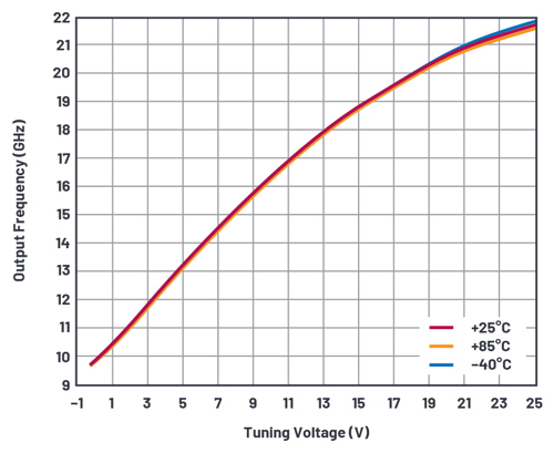
Figure 2. HMC733 tuning range.
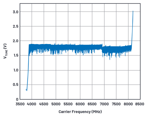
Figure 3. ADF4371 frequency vs. VTUNE.
PLL Improvements
The demand for higher data rates required lower error vector modulation (EVM) rates (Figure 4), which were dominated by the in-band phase noise contribution of a PLL synthesizer in a narrow-band wireless application, the high N required (9000) for a 1.8 GHz output using a 200 kHz channel raster meant a severe in-band penalty due to the 20log(N) contribution of the N divider. Higher order modulation rates such as 64 QAM demanded lower EVM, which drove the development, adoption, and deployment of fractional-N synthesizers like the ADF4153A and ADF4193, which decoupled the channel raster from the PFD frequency, meaning that the in-band noise was significantly reduced. The benefits of this are visible in a comparison between the ADF4106 to the ADF4153A (compare Figure 5 and Figure 6), in which the in-band noise at 1 kHz improves from –90 dBc/Hz to –105 dBc/Hz. This calculation was performed using ADIsimPLL™, which simulates all of Analog Device’s PLL offerings.
Fractional-N came with the additional benefit of faster acquisition times due to the wider allowable loop bandwidths, permitted with higher PFD frequencies. Fractional-N spurs were reduced to acceptable levels with various charge pump offset currents and sigma-delta dither functions. The ADF4193 and ADF4153A supported PFD frequencies of 26 MHz and 32 MHz, respectively, and still higher PFD frequencies permit users to further reduce N, which improves EVM further and eases frequency planning due to the lower occurrence and impact of integer boundary spurious (IBS). Recent PLL topologies available on the ADF4371 support PFD frequencies of up to 160 MHz. Improvements to fractional-N frequency resolution in which the fractional modulator increased from 12 bits of resolution to 39 bits of resolution also meant that PLLs could be used to generate almost any frequency with millihertz (mHz) of resolution and exact frequency accuracy.
A significant barrier to using fractional-N in the past was the presence of large fractional spurs, generated by the sigma-delta modulator—which degraded the spectral purity—the effect of which required additional engineering effort on behalf of the user to reduce or mitigate. Due to the low level of fractional spurious on the ADF4371, absent away from an integer boundary, the clean spectrum means that less time is spent investigating, debugging, or somehow mitigating the effects of these troublesome artifacts of frequency generation. The low level of in-band integer boundary spurious (–55 dBc) means that once filtered by the PLL filter, the spur is well attenuated. For example, if a 40 kHz filter is used with a 400 kHz channel raster, then the 35 dB of attenuation provided by the filter means the spur at the nearest channel to the integer boundary appears at –90 dBc. The ability to use high PFD frequencies up to 160 MHz means that integer boundaries occur less—five times less with a 160 MHz PFD frequency than with a 32 MHz PFD frequency.
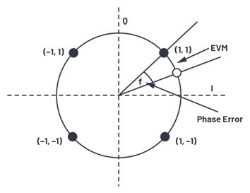
Figure 4. Phase error QPSK.
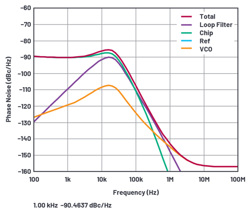
Figure 5. Integer-N, ADF4106 with VCO-1901846T.
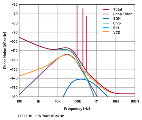
Figure 6. Fractional-N, ADF4153A with VCO-1901846T.
The ability to increase PFD frequency and frequency resolution was accompanied by improvements to the PLL figure of merit (FOM), evolving from –216 dBc/Hz on the ADF4153 to –233 dBc/Hz (frac mode) on the ADF4371. A comparison of the ADIsimPLL graphs in Figure 5 displaying the ADF4106 generating 1.85 GHz output, setup for 200 kHz PFD frequency in integer mode with a loop bandwidth of 10 kHz, to that of the ADF4371 setup for a PFD of 160 MHz and a loop bandwidth of 150 kHz. A 20 dB difference at a 1 kHz offset is observed, highlighting the progress in PLL synthesizer technology.
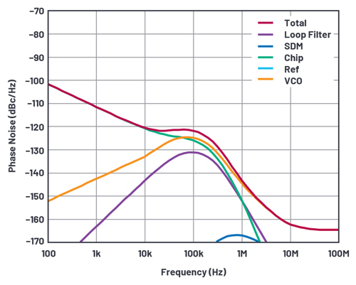
Figure 7. ADF4371.
A difference of integrated rms phase jitter from 1 ps to 51 fs is also shown. A notable observation is that in contrast to the past in which the inductor Q dominated the rms noise performance, the greatly improved in-band noise— enabled by lower FOM and fractional-N—allows the user to increase the loop filter bandwidth to 150 kHz, suppressing any VCO noise inside this bandwidth, and lessening the degradation present in the 10 kHz to 100 kHz range, which typically dominates the rms noise. A higher specification PLL reference source is essential in achieving this improved in-band phase noise, but the performance and flexibility improvements of such an approach mean this trade-off is acceptable to the majority of users. In some cases, the lower in-band noise of newer fractional-N PLLs competes with that enabled by offset or translation loop PLLs, in which a mixer is used in the feedback path from VCO to PFD, greatly simplifying frequency generation for all but the most demanding of applications.
The fundamental range of the ADF4371 VCO is from 4 GHz to 8 GHz, which is the sweet spot with respect to the VCO phase noise performance of the SiGe process used to fabricate the device. To generate higher frequencies, multipliers are used. Redesigning the VCO for double the frequency range is somewhat problematic, as the noise degrades by more than the 6 dB expected from scaling up the frequency range of the VCO. Hence, a frequency doubler is included, which extends the VCO range to 8 GHz to 16 GHz, together with a quadrupler, which extends the 4 GHz to 8 GHz VCO range to 16 GHz to 32 GHz. In each case, the multiplier generates some unwanted products, including the VCO feedthrough, along with 2×, 3×, and 5× the VCO frequency. To ease the filtering requirement, each multiplier circuit contains tracking filters that tune the output, which has the effect of maximizing the power of the wanted frequency against that of the unwanted products. Subharmonic suppression is typically as low as 45 dB from the doubled output and 35 dB from the quadrupled output.
Wideband Operation
The superiority of the newer PLL/VCO technology is obvious from the narrow-band example previously shown, but even more significant improvements can also be seen for wideband frequency generation using ADF4371 and comparing this to using the HMC704 PLL with the HMC733 VCO. The user faces many challenges with the discrete solution, in which the goal is to generate a clean variable LO from 20 GHz to 29 GHz.
- First, the HMC733 VCO output power must be split on board and divided down to a frequency suitable for the HMC704, so an external frequency divider (HMC492) must be used to scale the 10 GHz to 5 GHz range down to 5 GHz to 7.25 GHz permitted to the HMC704.
- A frequency doubler (HMC576) must then be used to multiply the 10 GHz to 15 GHz range up to 20 GHz to the 30 GHz range.
- An active low-pass filter is required to generate the required tuning voltage for the HMC733. This example uses the ADA4625-1. This also requires that the supply voltage to the op amp generates sufficient tuning voltage range (15 V in this instance).
- Variations in the tuning sensitivity must be compensated over the range of the VCO. Typically this is done by adjusting the charge pump current to maintain the product of charge pump gain and VCO gain.
- VCO feedthrough after the HMC576 multiplier is about –20 The tuning filter on the ADF4371 suppresses unwanted multiplier products by 35 dBc. This greatly simplifies any subsequent filtering.
By contrast the ADF4371 PLL/VCO generates this frequency range out of the box, requiring only an external high quality reference. The layout can be copied from the EV-ADF4371SD2Z, with the accompanying power management solution duplicated. The loop filter design is also greatly simplified, as variations in sensitivity kV do not require compensation from the end user, and an active filter element is not required. Instead of spending weeks on part selection and significant time developing simulation models for each discrete component, the user can use ADIsimPLL to design and simulate the expected performance and know exactly what to expect by evaluating the evaluation board of the ADF4371, which will very closely match the simulated performance. The lower component count and higher integration level presents obvious benefits to the size and weight of the system, but a significant performance improvement is also noted, as the calculated integrated rms jitter for the ADF4371 is 60 fs, as compared to 160 fs for the discrete solution. The component and area saving are obvious from the block diagram in Figure 9, and the total area of the active devices and the power splitter equals 96 mm2—omitting the necessary decoupling capacitors and other required passives—as compared to 49 mm2 for the ADF4371. The user can also opt for a 3.3 V supply to the VCO to save power if desired.
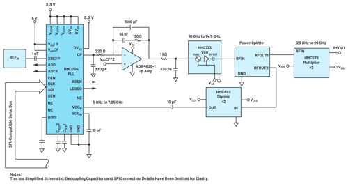
Figure 8. Discrete PLL/VCO multiplier solution.
Fig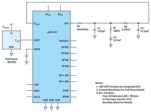 ure 9. ADF4371 block diagram.
Table 1. Size, Power, and Performance Comparison of Discrete PLL/VCO and Multipliers with ADF4371
|
|
Discrete PLL/VCO Multiplier Solution |
ADF4371 |
|
Active Component Count |
5 |
1 |
|
Output Frequency Range (GHz) |
20 to 29 |
16 to 32 |
|
Power Consumption (W) |
1.42 |
1.83 (5 V VCO rail)/ 1.4 (3.3 V VCO rail) |
|
Subharmonic Suppression (dBc) |
–20 |
–35 |
|
RMS Jitter ((1 kHz to 100 MHz)/fs) |
160 |
60 |
|
IC Component Area (Including Power Splitter) (mm2) |
96 |
49 |
For fundamental VCO mode, the spectral purity of the ADF4371 is at its highest, with unwanted spurious (non-inband) limited to harmonics of the VCO. For many converter clock applications, the square wave nature is not problematic and may indeed be desirable, but for instrumentation applications, wideband spurious frequencies must typically be below 50 dBc. Tuneable harmonic filters can assist with the removal of these harmonics, and the specially designed ADMV8416/ ADMV8432 are ideally suited to filtering the outputs of the ADF4371.
The ADMV8432 is a tuneable band-pass filter with a specified center frequency range of operation from 16 GHz to 32 GHz, a typical 3 dB BW of 18%, typical insertion loss of 9 dB, as well as wideband rejection greater than 30 dB. It was designed specifically for use with the ADF4371 quadrupler output. Likewise, the ADMV8416 is a tuneable band-pass filter operating from 7 GHz to 16 GHz, with typical 3 dB BW of 16%, typical insertion loss of 8 dB, and wideband rejection greater than 30 dB, intended for use with the ADF4371 doubler output.

Figure 10. ADF4371 20 GHz output.
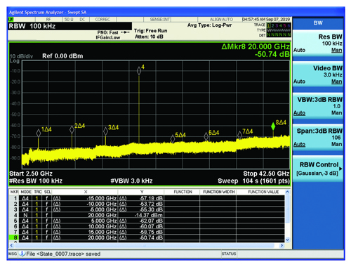
Figure 11. ADF4371 20 GHz output using the ADMV8432 filter.
Both the ADMV8416/ADMV8432 incorporate a dual overlapping band architecture with internal RF switches, which allows for wider frequency coverage while maintaining excellent rejection capability. The selection of the band is by digital logic control into a necessary level shifter. The level shifter ensures that the internal RF switches are biased accordingly for an optimum input third-order intercept (IIP3) of greater than +34 dBm.
Within each band of operation, the tuneable filters are controlled by means of an analog control voltage from 0 V to 15 V, which draws less than 1 µA of current. The generation of this control voltage is typically by means of a DAC and op amp driver circuit. An example of this is the AD5760 DAC followed by the ADA4898 op amp, which produces a relatively fast tuning speed and low noise driving voltage for the filters. If tuning speed is not critical, then the DAC can be driven directly into the tuning port of the filters.
Given the performance metrics of these analog tuneable filters, they can remove unwanted harmonic content from the ADF4371 synthesizer doubler and quadrupler outputs at a slight expense in output power. While additional stages of amplification may be necessary to overcome the insertion loss, the filters are generally smaller than a discrete switched bank solution, in particular where wideband tunability is needed. Additionally, the spurious levels of the synthesizer are typically improved from –35 dBc prior to filtering to a level of –55 dBc afterwards. Coupling of the unfiltered unused output can have an effect on the feedthrough and should be carefully modeled to get the full stop-band rejection of the filter IC.
Conclusion
The evolution in frequency generation involving various innovations in process, circuit, and packaging technologies provides users with greater functionality and performance in a smaller form factor than previous discrete solutions. Trends toward wideband frequency operation have provided the necessary impetus to develop ICs that cover several octaves for frequency ranges up to 32 GHz. The flexibility and simplicity enabled by the wideband PLLs/VCOs greatly shorten design time and time to market for the end customer.
Demand for spectral purity has driven innovations in filtering ICs that pair with these newly developed synthesizer ICs providing low phase noise, highly spectrally pure millimeter wave signal sources for the demands of modern wireless applications. The free simulation tool ADIsimPLL enables a user to evaluate and compare PLL performance, assisting with component choice with an easy to use, intuitive interface, and fast behavioral models. This tool saves considerable time on the part of the design engineer who would otherwise need to develop many differing mathematical models in many different domains to predict performance.
About the Authors
Ian Collins graduated from University College Cork with a degree in electrical and electronic engineering, and has worked in the RF and Microwave Group at Analog Devices since 2000. He is currently an applications manager in the Microwave Frequency Generation Group, which focuses mainly on phase-locked loop (PLL) and voltage controlled oscillator (VCO) products. When not spending time at work or with his young family, Ian enjoys photography and the theatre (both on- and off-stage), reading, and listening to music. He can be reached at ian.collins@analog.com.
David Mailloux is a product applications engineer within the RF and Microwave business unit at Analog Devices. He received both a Bachelor and Master of Science degree in electrical engineering from the University of Massachusetts Lowell in 2010 and 2012, respectively.
From 2010 to 2015, his experience includes working for Hittite Microwave and Symmetricom (now Microchip Technology). He has experience designing oscillators both at the semiconductor and the module level, and his theoretical background is complemented by adept laboratory practices.
In 2015, he joined ADI as a product applications engineer supporting highly integrated up/downconverters, as well as tunable filter products. Additionally, his technical support areas have included voltage controlled oscillators, phase-locked loops, frequency dividers, and frequency multipliers. He can be reached at david.mailloux@analog.com.
This article highlights the advances in microwave circuit design in recent years, which now mean that low phase noise VCOs on silicon technology can cover an octave range of frequency. Integrated output dividers on the same IC permit several octaves of lower frequency coverage, and multipliers allow frequencies as great as 32 GHz to be generated using a single IC. Advances in fractional-N PLL synthesizers now mean that overall rms jitter at microwave frequencies can be as low as 60 fs, with infinitesimal frequency resolution and minimal spurious tones. Low insertion loss wideband filters can be used with these integrated PLL/VCO ICs to improve the spectral performance of the entire system, greatly simplifying the challenge of microwave and millimeter wave local oscillator generation.


Glasgow trial explores AR cues for autonomous road safety
They've ploughed into a few vulnerable road users in the past. Making that less likely will make it spectacularly easy to stop the traffic for...