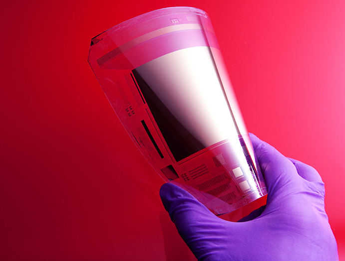
The discovery of Dr Freddie Withers of Exeter University and his colleagues is related to manufacturing very small electronic devices using two-dimensional materials, which would have the additional property of flexibility along with their compactness. It involves assemblies of single atom thick crystalline materials such as graphene.
The issue that Withers is addressing is the construction of semiconductor logic gates – the basic component of all computing systems which allow current to flow under some conditions but not others, thereby enabling “on or off” digital operations. These depend on insulators that can block the flow of electrons, but as devices get smaller, insulator layers have become so thin that electrons can leak through them via quantum mechanical effects. Therefore, researchers have been looking at replacing insulators with oxides that have a high dielectric constant (known as high-k). Such materials can store large amounts of electrical energy in an electric field, and therefore can act as better electrical insulators when they are very thin. However, current methods for depositing high-K materials are not compatible with two-dimensional materials.
Withers’ team has developed a method for embedding and patterning multifunctional high-K oxides within two-dimensional materials. It particularly focuses on a route to embed ultra-thin hafnium oxides within structures made from two-dimensional materials. The method depends on oxidation of hafnium disulphide (HfS2), a semiconductor with a layered structure. The team placed a flake of HfS2 a few layers thick within a stack of two-dimensional materials where the high-K dielectric is required, and irradiates the flake with visible laser light. This causes a transfer of charge within the semiconductor and atmospheric water, which leads to oxidation, converting it into a hafnium oxide.
“The fact we start with a layered 2D semiconductor and convert it chemically to its oxide using laser irradiation allows for high quality interfaces which improve device performance,” Withers said.
“What’s especially interesting for me is we found this oxidation process of the parent HfS2 to take place under laser irradiation even when its sandwiched between two neighbouring 2D materials. This indicates that water needs to travel between the interfaces for the reaction to occur.”
To test the technique, the team fabricated graphene-based field-effect transistors using hafnium oxide as a “gate” material. As they explain in a paper in Science Advances, these components match the performance of existing FETs but have the added advantage of flexibility. This new technique allows for the creation of a host of fundamental nano-electronic and opto-electronic devices including dual gated graphene transistors, and vertical light emitting and detecting tunnelling transistors, the team claims.
Swiss geoengineering start-up targets methane removal
No mention whatsoever about the effect of increased methane levels/iron chloride in the ocean on the pH and chemical properties of the ocean - are we...