This substrate platform could be used in both faster conventional complementary metal-oxide semiconductor (CMOS) electronics, as well as the emerging field of optoelectronics.
The computer industry is currently awaiting the next generation of microprocessors, which are likely to incorporate 3D elements, with so-called ‘fin’ structures.
By increasing surface area, they will be more conductive and powerful and also consume less power compared with conventional ‘planar’ chips. However, these chips are not inherently 3D, but rather comprised of stacked layers of separate chips.
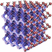
Researchers at the University of Twente have now developed a method for making true 3D structures out of silicon. First they etch millions of tiny holes, 300 nanometres in diameter and around eight micrometres in depth, into the upper surface of a wafer of silicon, then tilt it and repeat the etching process.
In order to obtain the required architecture throughout, the second step has to be aligned extremely accurately relative to the first, with a maximum permissible deviation of just 30 nanometres and half a degree.
‘It looks very simple to see how it’s done, but it took us 11 years to get it working and to measure the effect,’ said project lead Dr Willem Tjerkstra of Twente.
‘We use a plasma and the ions in that can be accelerated using an electric field to a very fast speed. They bombard the wafer and basically chip out parts of it.’
The 3D structures created in this way have tiny pores that intersect at an angle of 90°, resulting in a structure resembling that of a diamond crystal but larger by a factor of 2,000.
This is crucial, because the structure behaves as a semiconductor for light — with large photonic band gaps — making it possible to manipulate light in all sorts of different ways, for instance, trapping light or creating zones that are impenetrable to light of specific wavelengths.
‘If you remove, for instance, one of the pores in this structure then you have made a waveguide and because everywhere around this is photonic crystal, the light cannot exit the waveguide — you can also guide the light around corners very efficiently,’ Tjerkstra said.
Red Bull makes hydrogen fuel cell play with AVL
Formula 1 is an anachronistic anomaly where its only cutting edge is in engine development. The rules prohibit any real innovation and there would be...