The cloak - developed by a team from the US Department of Energy’s Lawrence Berkeley National Laboratory (Berkeley Lab) and the University of California (UC) Berkeley - is said to be microscopic in size but the principles behind the technology should enable it to be scaled-up.
Working with brick-like blocks of gold nanoantennas, the Berkeley researchers fashioned a so-called ’skin cloak’ 80nm thick that was wrapped around a 3D object the size of a few biological cells and arbitrarily shaped with multiple bumps and dents.
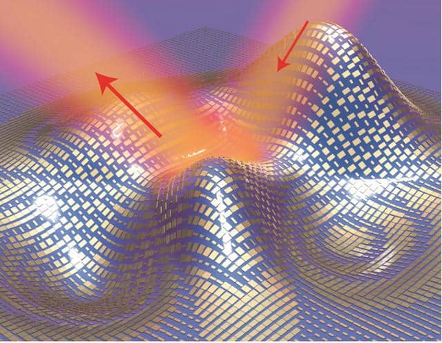
According to a statement, the surface of the skin cloak was meta-engineered to reroute reflected light waves so that the object was rendered invisible to optical detection when the cloak is activated.
“This is the first time a 3D object of arbitrary shape has been cloaked from visible light,” said Xiang Zhang, director of Berkeley Lab’s Materials Sciences Division. “Our ultra-thin cloak now looks like a coat. It is easy to design and implement, and is potentially scalable for hiding macroscopic objects.”
Zhang is the corresponding author of a paper - An ultra-thin invisibility skin cloak for visible light - describing the research in Science. Xingjie Ni and Zi Jing Wong are the lead authors. Other co-authors are Michael Mrejen and Yuan Wang.
The scattering of light from its interaction with matter enables us to detect and observe objects. The rules that govern these interactions in natural materials can be circumvented in metamaterials whose optical properties arise from their physical structure rather than their chemical composition.
Zhang and his research group have spent the last decade pushing the boundaries of how light interacts with metamaterials, and have managed to curve the path of light or bend it backwards to render objects optically undetectable. Formerly, their metamaterial-based optical carpet cloaks were bulky and hard to scale-up, and entailed a phase difference between the cloaked region and the surrounding background that made the cloak itself detectable.
“Creating a carpet cloak that works in air was so difficult we had to embed it in a dielectric prism that introduced an additional phase in the reflected light, which made the cloak visible by phase-sensitive detection,” said Ni. “Recent developments in metasurfaces, however, allow us to manipulate the phase of a propagating wave directly through the use of subwavelength-sized elements that locally tailor the electromagnetic response at the nanoscale, a response that is accompanied by dramatic light confinement.”
In the Berkeley study, when red light struck an arbitrarily shaped 3D sample object measuring approximately 1,300 square microns that was conformally wrapped in the gold nanoantenna skin cloak, the light reflected off the surface of the skin cloak was identical to light reflected off a flat mirror, making the object underneath it invisible, even by phase-sensitive detection. The cloak can be turned “on” or “off” by switching the polarisation of the nanoantennas.
“A phase shift provided by each individual nanoantenna fully restores both the wavefront and the phase of the scattered light so that the object remains perfectly hidden,” said Wong.
Future outcomes from this field of research include high-resolution optical microscopes and superfast optical computers. Furthermore, invisibility skin cloaks on the microscopic scale might prove valuable for hiding the detailed layout of microelectronic components or for security encryption purposes.


Red Bull makes hydrogen fuel cell play with AVL
Formula 1 is an anachronistic anomaly where its only cutting edge is in engine development. The rules prohibit any real innovation and there would be...