Creating thin photovoltaic cells has long been a goal of researchers working in the field of crystalline silicon. Thinner cells can be semi-transparent or flexible, making them more versatile than thick cells, and also they use less material, reducing the cost of the cells. But reducing the thickness is fraught with difficulty. Cutting a thin layer from a block of silicon causes loss of material, known as kerf loss. Moreover, thinner silicon films absorb less light than thicker ones; photons, especially ones at longer light wavelengths, can pass straight through the film before their energy is absorbed.
The new research brings together a team drawn from different disciplines within the photovoltaic community to tackle these problems. “The core of this project was to bring together researchers from the different fields needed (photovoltaics, photonics, nanostructuring) to interact directly,” explained research leader Valerie Depauw of imec, a nanoelectronics and digital technologies R&D hub in Leuven, Belgium.
The team used a “kerf-less” method to create a thin film, known as the “empty-space-in-silicon” technique. This involves etching an array of narrow pits onto the surface of a piece of crystalline silicon. Heat treatment causes silicon at the edges of these pits to “heal over”, while below this healed surface the pits join up, creating a void below a thin film of crystalline material. The thin layer remaining above the void can undergo surface treatment before being bonded to a low-cost substrate and removed.
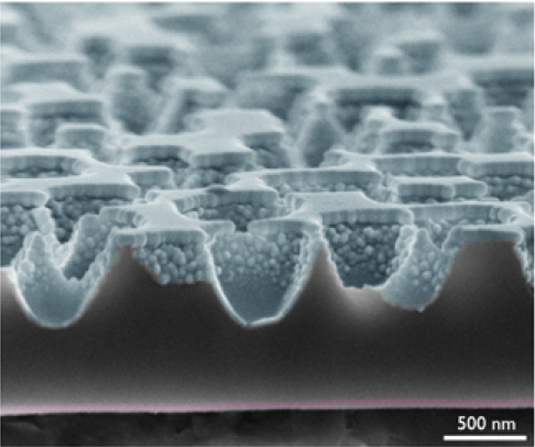
Previous research has shown that creating a non-regular pattern on the surface of crystalline silicon can improve its light-absorbing capability. In a paper in NanoFutures, the team explains that patterns including gentle slopes work best. The team used a process called reactive ion etching to create a pattern using a mask made from a self=-assembled layer of charged polystyrene beads, resulting in a surface shaped with shallow, rounded ‘nanocups’. This has two advantages over previous patterning processes, they explain; it wastes less material, and improves light capture.
The resulting photovoltaic cell has an effective thickness of 830nm and an efficiency of 8.6 per cent, the team claimed. “The main applications of our thin crystalline-Si solar cells could be in buildings as windows and skylights, where they will bring more freedom for integration, and possibly lighter and thinner module designs,” said Depauw.


Red Bull makes hydrogen fuel cell play with AVL
Many a true word spoken in jest. "<i><b>Surely EVs are the best solution for motor sports</b></i>?" Naturally, two electric motors demonstrably...