The research, at the engineering department of Columbia University in New York City, centred around an attempt to reproduce the electronic structure of graphene in a synthetic semiconductor device.
Graphene’s potential is derived from the way its electrons behave; carbon has four electrons available for bonding, and in graphene, three of them bind each carbon atom strongly to its neighbours to form the characteristic flat hexagonal lattice, but the fourth is free to move along the plane, giving the material its outstanding electrical conductivity. But one problem engineers have encountered in exploiting this property is that the properties depend on this specific configuration of carbon; it cannot be altered to create different conductive effects.
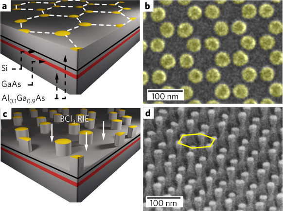
The Columbia team, led by physicist Prof Aron Pinczuk, used the technology normally employed to manufacture microprocessors to engineer graphene-like behaviour in gallium arsenide, a common industrial semiconductor.
Working with colleagues at Princeton and Purdue Universities and the Italian Institute Of Technology in Genoa, they devised a method using nanothithography and etching to create a hexagonal pattern of “quantum wells", which confine the movement of electrons to a lateral direction, onto a sheet of GaAs. The dots were placed about 50nm apart, which is much further than the atoms in graphene but close enough for them to interact quantum mechanically, effectively sharing their electrons like atoms do in solids.
In a paper in Nature Nanotechnology, the team describe the technique and how they tested it. To confirm that electrons behaved like those of graphene, they illuminated the quantum well sites with a laser, and measured how the light was scattered. This scattering showed a loss of energy in the light that corresponded to the transitions caused by electrons ascending through quantum energy levels, as they do in atoms. When they mapped these transitions, the team found that they were approaching zero in a linear fashion around what is called the “Dirac point” where the electron density vanishes, a hallmark of graphene.
The ability to recreate graphene’s electronic behaviour opens up new avenues for engineering, the team claims, because changing the pattern and distribution of the quantum dots would modulate the electrons’ behaviour. Moreover, the greater-than-atomic spacing of the dots would allow engineers to create even more exotic quantum behaviour by applying magnetic fields to the material.
“This work is really a major advance in artificial graphene. Since the first theoretical prediction that system with graphene-like electronic properties may be artificially created and tuned with patterned 2D electron gas, no one had succeeded, until the Columbia work, in directly observing these characteristics in engineered semiconductor nanostructures,” said Prof. Steven G. Louie, a physicist at the University of California, Berkeley, commenting on the research.
Columbia team member Dr Shalom Wind commented: “This is a rapidly expanding area of research, and we are uncovering new phenomena that couldn’t be accessed before. As we explore novel device concepts based on electrical control of artificial graphene, we can unlock the potential to expand frontiers in advanced optoelectronics and data processing.”
Team leader Pinczuk added: ”What was really critical to our work was the impressive advancements in nanofabrication. These offer us an ever-increasing toolbox for creating a myriad of high-quality patterns at nanoscale dimensions. This is an exciting time to be a physicist working in our field.”


Glasgow trial explores AR cues for autonomous road safety
They've ploughed into a few vulnerable road users in the past. Making that less likely will make it spectacularly easy to stop the traffic for...