Photonic chips made from silicon will play a major role in future optical networks for worldwide data traffic.
The high refractive index of silicon makes optical structures the size of a fraction of the diameter of a human hair possible and by squeezing more and more optical structures for light distribution, modulation, detection and routing into smaller chip areas allows for higher data rates at lower fabrication costs.
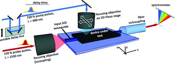
As the complexity of optical chips increases, testing and characterising such chips becomes more difficult. Light traveling in the chip is confined in the silicon, that is, it cannot be ‘seen’ or measured from the outside.
Southampton researchers are now said to have now developed a new method, which will help solve this problem, to find out at which time the light in the chip is at which position.
The technique - Ultrafast photomodulation spectroscopy (UPMS) - uses ultraviolet laser pulses of femtosecond duration to change the refractive index of silicon in a minute area on the photonic chip.
Non-contact characterisation tools like UPMS are vital for scientist designing complex photonic chips as the UPMS technique is fast, robust and has the potential to be used for industrial testing in the photonics industry.
The research is published in the latest issue of the journal Nature Photonics.
In a statement Dr Roman Bruck, from Physics and Astronomy at Southampton University and lead author of the study, said: ‘Monitoring the transmission of the chip while the refractive index is locally changed gives a precise picture of how the light flows through it.
‘This allows testing of individual optical elements on the chip, a crucial step in the design optimisation to ensure its flawless operation. Because the changes induced by the technique are fully reversible, this testing method is non-destructive and after testing, the chip can be used for its intended application.’
The research team, from Physics and Astronomy and the Optoelectronics Research Centre (ORC) at the University, expects to establish the technique as a standard characterisation tool, making photonic chips under development more reliable and bringing them into the market quicker.
The work has been funded by the Engineering and Physical Sciences Research Council (EPSRC).


Glasgow trial explores AR cues for autonomous road safety
They've ploughed into a few vulnerable road users in the past. Making that less likely will make it spectacularly easy to stop the traffic for...