Researchers have developed a new fabrication technique that uses a single wafer to build a nearly infinite number of thin film electronic circuits that are peelable from a surface.
The technique from researchers at Purdue University and the University of Virginia is claimed to eliminate several manufacturing steps and associated costs, and allows any object to sense its environment or be controlled through the application of a high-tech sticker.
According to Purdue, the stickers could eventually facilitate wireless communication. The researchers demonstrate capabilities on various objects in a paper recently published in the Proceedings of the National Academy of Sciences.
"We could customise a sensor, stick it onto a drone, and send the drone to dangerous areas to detect gas leaks, for example," said Chi Hwan Lee, Purdue assistant professor of biomedical engineering and mechanical engineering.
Electronic circuits are often individually built on their own silicon wafer, a flat and rigid substrate. The silicon wafer then withstands the high temperatures and chemical etching that are used to remove the circuits from the wafer.
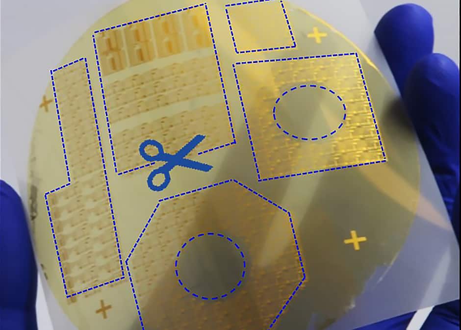
Lee’s new ‘transfer printing’ fabrication technique is claimed to cut down manufacturing costs by using a single wafer to build a nearly infinite number of thin films holding electronic circuits. Instead of high temperatures and chemicals, the film can peel off at room temperature with the help of water.
“It’s like the red paint on San Francisco’s Golden Gate Bridge – paint peels because the environment is very wet,” Lee said. “So in our case, submerging the wafer and completed circuit in water significantly reduces the mechanical peeling stress and is environmentally friendly.”
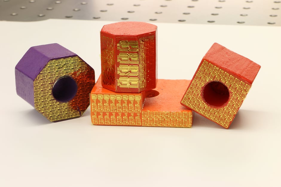
A ductile metal layer, such as nickel, inserted between the electronic film and the silicon wafer, makes the peeling possible in water. These thin-film electronics can then be trimmed and pasted onto any surface to give an object electronic features.
A sticker attached to a flower pot gave the object temperature sensing capabilities that could affect the plant’s growth. Lee’s lab also demonstrated that the components of electronic integrated circuits work just as well before and after they were made into a thin film peeled from a silicon wafer. The researchers used one film to turn on and off an LED light display.
“We’ve optimised this process so that we can delaminate electronic films from wafers in a defect-free manner,” Lee said.
This technology holds a non-provisional US patent.


Glasgow trial explores AR cues for autonomous road safety
They've ploughed into a few vulnerable road users in the past. Making that less likely will make it spectacularly easy to stop the traffic for...