A type of megapixel image sensor developed by scientists at Andor Technology in Northern Ireland, Fairchild Imaging in the US and PCO in Germany made its debut at the Laser Conference and Exhibition in Munich this week.
Since its inception, CMOS image sensor (CIS) technology has held great potential to become the detector of choice for many scientific imaging applications. These demanding fields require a unique combination of sensitivity, speed, dynamic range, resolution and field of view.
However, although CIS technology has steadily improved, it has not fully realised its potential, with charge-coupled device (CCD) and, more recently, electron-multiplying charge-coupled device (EMCCD) detectors remaining the choice for the majority of high-end scientific imaging applications.
That is because the performance of traditional CIS devices has generally been worse than CCDs and their acceptance into scientific markets has been limited owing to a reputation of unacceptably high read noise and dark current, lower fill factors and greater non-uniformity.
Unlike previous generations of CISs and CCD-based sensors, the three companies claim that their so-called sCMOS sensors will change all that: they will be extremely low noise and offer rapid frame rates, a wide dynamic range, a high quantum efficiency (QE), a high resolution and a large field of view.
While the primary technical advancements that underlie the sensor design are proprietary, the companies did disclose some of the architectural detail.
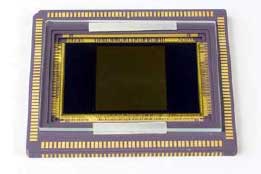
A 5.5-megapixel sCMOS sensor from Andor Technology based on the sCMOS process
The sensor features a split readout scheme in which the top and bottom halves of the sensor are read out independently. Each column within each half of the sensor is equipped with dual column level amplifiers and dual analogue-to-digital (ADC) converters designed to minimise read noise and maximise dynamic range simultaneously.
The dual column level amplifier/ADC pairs have independent-gain settings and the final image is reconstructed by combining pixel readings from both the high- and low-gain readout channels to achieve a wide intra-scene dynamic range from a small pixel pitch.
Each pinned-photodiode pixel has five transistors, enabling the use of a novel global shutter mode and also facilitating correlated double sampling (CDS) and a lateral anti-blooming drain.
The sensor is integrated with a microlens array that serves to focus much of the incident light per pixel away from the transistors and onto the exposed silicon, enhancing the quantum efficiency - a process that is analogous to the use of microlenses in interline CCDs to focus light away from column masks.
It is configured to offer low dark current and extremely low read noise with true CDS. Non-linearity is less than one per cent and is further correctable to less than 0.2 per cent.
The sensor also has anti-blooming of less than 10,000:1, meaning that the pixels can be significantly oversaturated without charge spilling into neighbouring pixels. It is also possible to use the anti-blooming capability to hold all or parts of the sensor in a state of ‘reset’, even while light is falling on these pixels.
The time to transfer charge after the exposure is complete is less than 1µssec, rendering the sensor useful for fast electronic shuttering and ‘double-exposure’ techniques such as particle imaging velocimetry (PIV).
A complete technical article on the sensor technology is available here.


Red Bull makes hydrogen fuel cell play with AVL
Formula 1 is an anachronistic anomaly where its only cutting edge is in engine development. The rules prohibit any real innovation and there would be...