Piezoelectric materials, which generate a voltage in response to mechanical deformation, are finding increasing numbers of applications in devices like accelerometers and energy harvesting from movement. However, until now it has not been possible to manufacture such materials in large sheets, which mean that they could be integrated directly onto silicon chips. Instead, separate components have to be embedded onto silicon substrates, increasing their manufacturing cost and limiting their more widespread usage.
Researchers from the Future Low Energy Technologies centre of excellence (FLEET) at the Royal Melbourne Institute of Technology have now developed a low-cost method to produce two-dimensional sheets of gallium phosphate, a quartz-like material used in piezoelectric pressure sensors since the 1980s. Particularly useful in the high-temperature applications, it has not previously been used as a two-dimensional material because it does not naturally crystallise in a layered structure.
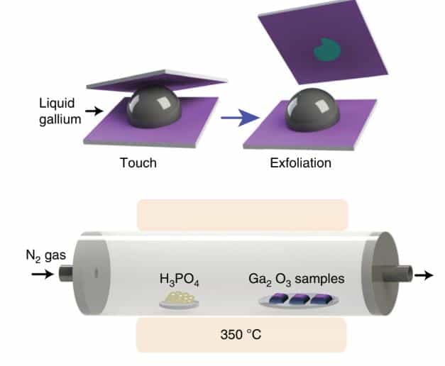
The FLEET team, led by Prof Kourosh Kalantar-zadeh, last year developed a technique for making two-dimensional materials based on dissolving metals in liquid metal, to create two-dimensional layers of oxides which did not previously exist as layered structures. They described this process in a paper in Science. "We adopted the liquid-metal material deposition technique we developed recently to create 2D films of GaPO4 through an easy, two-step process," said Prof Kalantar-zadeh.
The two steps involved are firstly, to exfoliate gallium oxide from the surface of liquid gallium, which is possible because the oxide does not have any affinity to the bulk of liquid metal. The second stage is to print that film onto a substrate and transform it into gallium phosphate by exposure to phosphate vapour. The team describes the process in a paper in Nature Communications. Prof Kalantar-zadeh has moved to the University of New South Wales since completing the research.
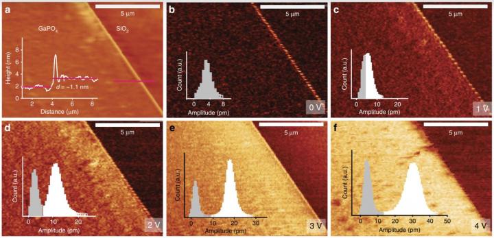
The process can be used to make gallium phosphate nanosheets with areas of several square centimetres and unit cell thickness. Testing this material with a piezo- force microscope showed it to have a high out of plane piezoelectric coefficient of 8 to 10 pm/V, sufficiently high to be suitable for piezoelectric sensing and energy harvesting, the team claims.


Project to investigate hybrid approach to titanium manufacturing
What is this a hybrid of? Superplastic forming tends to be performed slowly as otherwise the behaviour is the hot creep that typifies hot...