Joseph Lyding, a professor of electrical and computer engineering at the University of Illinois, led a group that developed a new microscope probe-sharpening technique. The technique is described in research published in the journal Nature Communications.
Scanning probe microscopes provide images of tiny structures with high resolution at the atomic scale. The tip of the probe skims the surface of a sample to measure mechanical, electrical or chemical properties.
Such microscopes are widely used among researchers who work with structures in fields from nanotechnology to cellular biology.
According to the university, labs can spend hundreds of thousands of dollars on an elegant instrument — for example, a scanning tunneling microscope (STM) or an atomic force microscope (AFM) — yet the quality of the data depends on the probe. Probes can degrade rapidly with use, wearing down and losing resolution. In such cases, the researcher then has to stop the scan and replace the tip.
To shape tips, researchers shoot a stream of ions at the tip. The material sputters off as the ions collide with the tip, whittling away the probe.
One day in the lab, after yet another tip failure, Lyding had the simple, novel idea of applying a matching voltage to the tip to deflect the incoming ions. When a voltage is applied to a sharp object, the electrical field gets stronger as the point narrows. Ions approaching the sharpest part of the electrified tip are deflected the most.
‘This causes the ions to remove the material around that sharp part, not on the sharp part itself, and that makes it sharper,’ said Lyding. ‘You preserve the point and you sharpen what’s around it.’
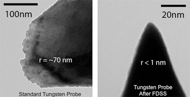
Lyding and graduate student Scott Schmucker purchased an inexpensive ion gun and tested Lyding’s idea. STM tips with a starting radius of 100nm were honed to a sharp 1nm point, yielding extremely high resolution.
In addition, the sputtering process is said to work with any electrically conductive material.
Lyding and Schmucker then teamed with University of Illinois chemistry professor Gregory Girolami and materials science and engineering professor John Abelson, whose groups had demonstrated coatings for silicon semiconductors made of a material called hafnium diboride.
The coatings are 10 times harder than the metal usually used to make STM tips, but are also metallic — the key property for the ion-sputtering process.
The group applied the hafnium diboride coatings to the probes, sputtered them further, and found that the resulting probes are stable, durable and excel in the types of microscopy and patterning applications for which such tips are used.
‘Nobody else makes probes with the combination of sharp, hard and metallic conduction,’ said Lyding, who is also affiliated with the Beckman Institute for Advanced Science and Technology at the University of Illinois. ‘You can find one or the other but not all three. There’s a tremendous demand for that.’
The researchers are now moving to commercialise their probes.
They received a patent and started a company called Tiptek to begin manufacture. They are also expanding their sharpening technique to include AFM probes as well as STM, and are developing batch-processing techniques for higher throughput.


April 1886: the Brunkebergs tunnel
First ever example of a ground source heat pump?