A new process has been developed for creating thin, small inorganic light-emitting diodes (LEDs) and assembling them into large arrays.
Applications for the arrays, which can be printed onto flat or flexible substrates ranging from glass to plastic and rubber, include general illumination, high-resolution home theatre displays, wearable health monitors and biomedical imaging devices.
'Our goal is to marry some of the advantages of inorganic LED technology with the scalability, ease of processing and resolution of organic LEDs,' said John Rogers, the Flory-Founder Chair Professor of Materials Science and Engineering at the University of Illinois.
Rogers and collaborators at the university developed the process with researchers at Northwestern University, the Institute of High Performance Computing in Singapore, and Tsinghua University in Beijing.
Compared to organic LEDs, inorganic LEDs are brighter, more robust and longer lived. Organic LEDs, however, are attractive because they can be formed on flexible substrates, in dense, interconnected arrays. The researchers’ new technology combines features of both.
'By printing large arrays of inorganic LEDs and interconnecting them using thin-film processing, we can create general lighting and display systems that otherwise could not be built in the conventional ways that inorganic LEDs are made, manipulated and assembled,' Rogers said.
To overcome requirements on device size and thickness associated with conventional wafer dicing, packaging and wire bonding methods, the researchers developed epitaxial growth techniques for creating LEDs with sizes up to 100 times smaller than usual. They also developed printing processes for assembling the devices into arrays on stiff, flexible and stretchable substrates.
As part of the growth process, a sacrificial layer of material is embedded beneath the LEDs. When fabrication is complete, a wet chemical etchent removes this layer, leaving the LEDs undercut from the wafer, but still tethered at anchor points.
To create an array, a rubber stamp contacts the wafer surface at selected points, lifts off the LEDs at those points, and transfers them to the desired substrate.
'The stamping process provides a much faster alternative to the standard robotic pick-and-place process that manipulates inorganic LEDs one at a time,' Rogers said. 'The new approach can lift large numbers of small, thin LEDs from the wafer in one step, and then print them onto a substrate in another step.'
By shifting position and repeating the stamping process, LEDs can be transferred to other locations on the same substrate. In this fashion, large light panels and displays can be crafted from small LEDs made in dense arrays on a single, comparatively small wafer.
And, because the LEDs can be placed far apart and still provide sufficient light output, the panels and displays can be nearly transparent. The thin device geometries allow the use of thin-film processing methods, rather than wire bonding, for interconnects.
In addition to solid-state lighting, instrument panels and display systems, flexible and even stretchable sheets of printed LEDs can be achieved. 'Wrapping a stretchable sheet of tiny LEDs around the human body offers interesting opportunities in biomedicine and biotechnology,' Rogers said.
Ford, the National Science Foundation and the US Department of Energy funded the work.
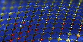
Stretchable micro-LED display consisting of an interconnected mesh of printed micro LEDs bonded to a rubber substrate


Swiss geoengineering start-up targets methane removal
No mention whatsoever about the effect of increased methane levels/iron chloride in the ocean on the pH and chemical properties of the ocean - are we...