Quantum sensing systems could be less cumbersome and applied more widely with a metasurface optical chip developed at the Birmingham University led UK Quantum Technology Hub.
Sensing devices have a range of industrial uses - from carrying out ground surveys to monitoring volcanoes – and scientists are developing ways to improve their sensitivity with quantum technologies that are based on cold atoms. Machines using quantum technology are, however, bulky and difficult to transport, making current designs unsuitable for most industrial uses.
Quantum sensor monitors cancer treatments with single photon
What to expect from the budding quantum industries
According to Birmingham University, the researchers have used a new approach that will enable quantum sensors to shrink to a fraction of their current size. The research was conducted by an international team led by Birmingham University and SUSTech in China in collaboration with Paderborn University in Germany. Their results are published in Science Advances.
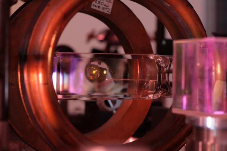
The quantum technology currently used in sensing devices works by finely controlling laser beams to engineer and manipulate atoms at super-cold temperatures. To manage this, the atoms have to be contained within a vacuum-sealed chamber where they can be cooled to the desired temperatures.
A key challenge in miniaturising the instruments is in reducing the space required by the laser beams, which typically need to be arranged in three pairs, set at angles. The lasers cool the atoms by firing photons against the moving atom, lowering its momentum and cooling it down.
The new findings show how a new technique can be used to reduce the space needed for the laser delivery system. The method uses devices optical metasurfaces that can be used to control light.
A metasurface optical chip can be designed to diffract a single beam into five separate, uniform beams that are used to supercool the atoms. This single chip can replace the complex optical devices that currently make up the cooling system.
Metasurface photonic devices have inspired a range of novel research activities in the past few years and this is the first time researchers have been able to demonstrate its potential in cold atom quantum devices.
Dr Yu-Hung Lien, lead author of the study, said: “The mission of the UK Quantum Technology Hub is to deliver technologies that can be adopted and used by industry. Designing devices that are small enough to be portable or which can fit into industrial processes and practices is vital. This new approach represents a significant step forward in this approach.”
The team have succeeded in producing an optical chip that measures 0.5mm across, resulting in a platform for future sensing devices measuring about 30cm cubed. The next step will be to optimise the size and the performance of the platform to produce the maximum sensitivity for each application.


Red Bull makes hydrogen fuel cell play with AVL
Surely EVs are the best solution for motor sports and for weight / performance dispense with the battery altogether by introducing paired conductors...