
Scientists there have made use of graphene’s unique properties to fashion new 2D designer materials that could be utilised to create light emitting devices for the next-generation of mobile phones, tablets and televisions that are incredibly thin as well as flexible, durable and even semi-transparent.
The team was led by Sir Kostya Novoselov, joint winner for the 2010 Nobel Prize for Physics for ground-breaking experiments with graphene, and the breakthrough was made by creating LEDs that were engineered on an atomic level, constructing them by combining 2D crystals made from varying materials.
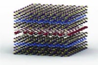
Being so thin, at only 10-40 atoms thick, the new components are capable of forming the basis for the first generation of semi-transparent smart devices, which emit light from across their whole surface. The components could be used to build heterostructures – stacked layers of various 2D materials – to create new possibilities for graphene-based optoelectronics, tailoring the devices’ capabilities by varying the materials used to make them. They could also be used to introduce new types of quantum wells to control the movement of electrons.
Novoselov said: ‘By preparing the heterostructures on elastic and transparent substrates, we show that they can provide the basis for flexible and semi-transparent electronics.
‘The range of functionalities for the demonstrated heterostructures is expected to grow further on increasing the number of available 2D crystals and improving their electronic quality.
‘The proof of principal has been demonstrated and the device worked nicely but there is still a long way to go. The LED comprises less than 10 atomic layers and is very flexible and bendable, and is semi transparent as it is so thin. It could one day be used for any applications requiring flexible, semi transparent lighting, whether this was a display or a regular light.
‘The technology is so different from the LED technology used today - it allows the inclusion of other elements into the LED by adding extra layers, and you could also put a logic circuit in this. I expect that the first application will be something unusual; a multifunctional device rather than a mobile phone screen.’
According to the research team, the LED structures are robust and have shown no significant change in performance over many weeks of measurements, while the quantum efficiency - the number of photons emitted per electron injected - is already comparable to that of organic LEDs. The technology builds on the discovery of one-atom thick graphene, which was first isolated and explored in 2004 at Manchester University.
‘There are three different directions to take with our next step,’ Novoselev explained. ‘We can combine more types of different materials to create more complex quantum wells, and we can explore the use of other materials so that the pool of materials used to make the heterostructures is bigger. The latter could possibly increase the efficiency of the devices or explore how we can change the colour they display. Finally, we will be looking at how to mass-produce the devices.’
At present, the researchers are not working with a commercial partner. However, they hope that - as with the case of previous developments around transistors and diodes in this field - industrial partners will soon show an interest in the work.


Glasgow trial explores AR cues for autonomous road safety
They've ploughed into a few vulnerable road users in the past. Making that less likely will make it spectacularly easy to stop the traffic for...