The breakthrough could open the door to a wide range of potential new applications, from phone displays and flatter screens to wearable technology.
The two main types of particle-based semiconductors already in use are colloidal quantum dots and organic semiconductors. These materials are at the nanoscale. Their tiny size means they are subject to a phenomenon known as quantum confinement, which causes changes to their optical and electronic properties. These changes make them suitable for their intended applications.
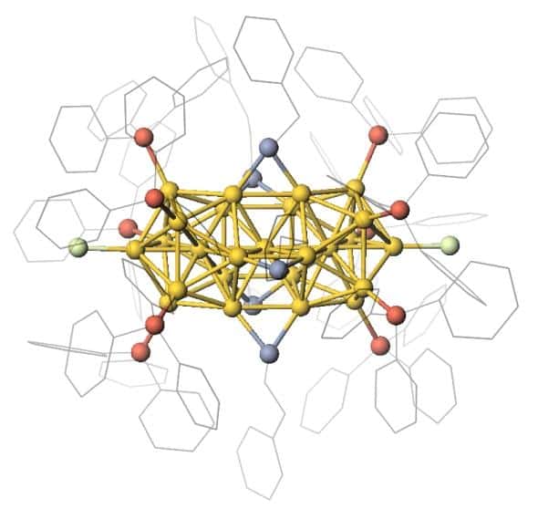
Metal nanoclusters combine aspects of both these other materials, but despite containing all of the right ingredients have never – until now - been shown to display semiconducting properties.
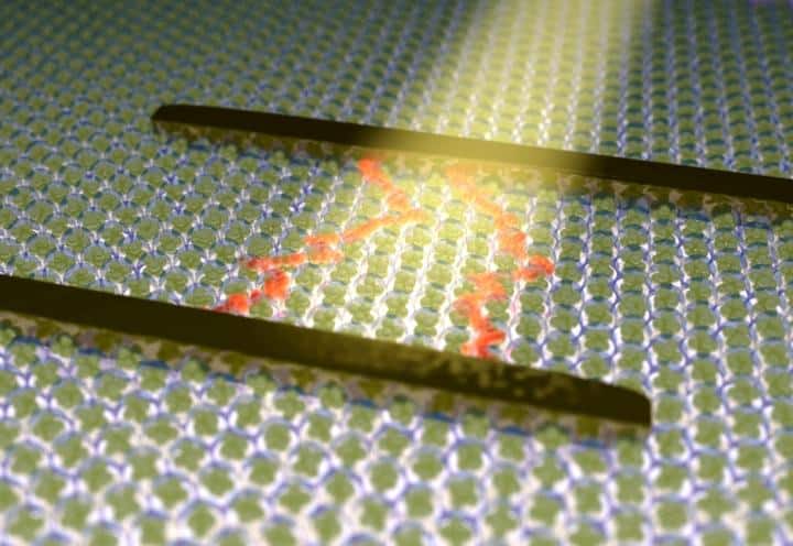
The team devised a way of making films of nanoclusters consisting of 25 gold atoms (Au25). They then observed that the nanoclusters displayed semiconducting properties. Specifically, they observed field effect and photoconductivity in phototransistors made of these films. These unique properties are hallmarks of all semiconducting materials.
Explaining the potential applications of this finding Professor Christian Klinke of Swansea University’s chemistry department said: "The discovery of semiconducting properties in metal nanoclusters could pave the way for a variety of new applications, from field effect transistors and photodetectors to light emitting diodes and solar cells…. We need to build on this finding and refine the technique further. But this discovery points the way ahead. It shows that we can use metal nanoclusters to produce high quality semiconducting films that are easy to assemble."
Outlining other potential applications Dr Andrés Black of the University of Hamburg said: "The affinity of the metal core to different molecular functionalities could make them highly sensitive gas sensors". His Hamburg colleague Michael Galchenko added: "The integration with other low dimensional materials could yield heterostructures with new and interesting functionalities."
The findings were published in Advanced Materials.


Nanogenerator consumes CO2 to generate electricity
Whoopee, they've solved how to keep a light on but not a lot else.