Graphene has numerous properties including flexibility, transparency, high-strength, and conductivity - both thermal and electrical – that is 10 times better than copper.
The material was first isolated at Manchester University by Andre Geim and Kostya Novoselov in 2004, earning them the Nobel Prize for Physics in 2010.
Applications identified for graphene include flexible electronics, more powerful computer chips and solar panels, water filters and bio-sensors but its performance has been mixed and industry adoption slow.
Now a study published in Nature Communications identifies silicon contamination as the cause of disappointing results and details how to produce higher performing, pure graphene.
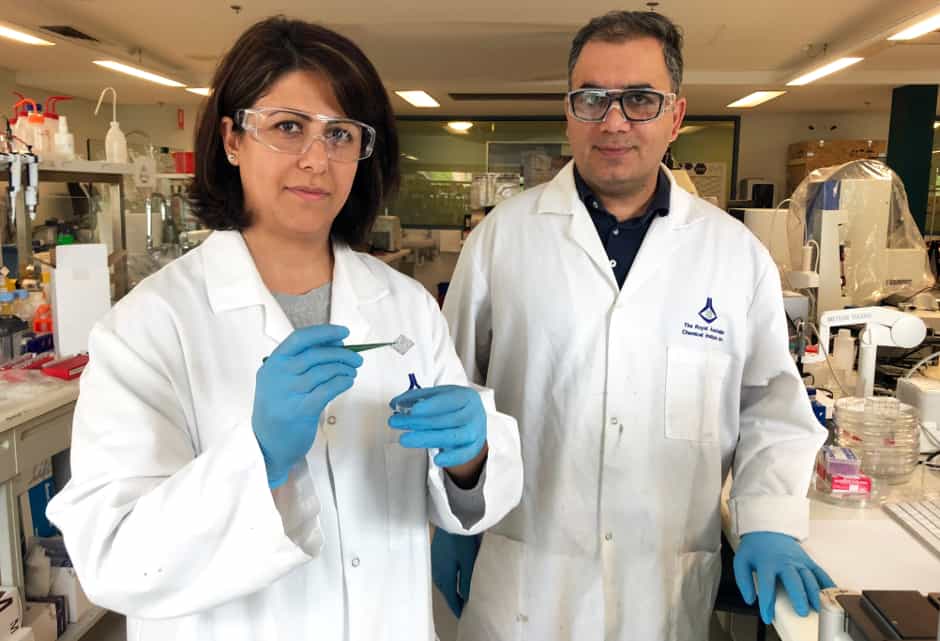
The RMIT University team led by Dr Dorna Esrafilzadeh and Dr Rouhollah Ali Jalili inspected commercially-available graphene samples with a scanning transition electron microscope.
"We found high levels of silicon contamination in commercially available graphene, with massive impacts on the material's performance," Esrafilzadeh said.
According to RMIT, tests found that silicon present in natural graphite, the raw material used to make graphene, was not being fully removed when processed.
"We believe this contamination is at the heart of many seemingly inconsistent reports on the properties of graphene and perhaps many other atomically thin 2D materials,” Esrafilzadeh said.
"Graphene was billed as being transformative, but has so far failed to make a significant commercial impact, as have some similar 2D nanomaterials. Now we know why it has not been performing as promised, and what needs to be done to harness its full potential."
The testing also demonstrated the major influence contaminants have on performance, with contaminated material performing up to 50 per cent worse when tested as electrodes.
"This level of inconsistency may have stymied the emergence of major industry applications for graphene-based systems. But it's also preventing the development of regulatory frameworks governing the implementation of such layered nanomaterials, which are destined to become the backbone of next-generation devices," she said.
The two-dimensional property of graphene sheeting, which is only one atom thick, makes it ideal for electricity storage and new sensor technologies that rely on high surface area.
The RMIT study reveals how that 2D property is also graphene's Achilles' heel, by making it vulnerable to surface contamination, and underscores how important high purity graphite is for the production of more pure graphene.
Using pure graphene, researchers demonstrated how the material performed extraordinarily well when used to build a supercapacitor.
When tested, the device's capacity to hold electrical charge was the largest so far recorded for graphene and within sight of the material's predicted theoretical capacity.
In collaboration with RMIT's Centre for Advanced Materials and Industrial Chemistry, the team then used pure graphene to build a humidity sensor with the highest sensitivity and the lowest limit of detection ever reported.
"We hope this research will help to unlock the exciting potential of these materials."


Swiss geoengineering start-up targets methane removal
No mention whatsoever about the effect of increased methane levels/iron chloride in the ocean on the pH and chemical properties of the ocean - are we...