One of the most interesting areas of research into two-dimensional materials is how they behave when they are stacked together.
The best known of these materials is graphene, but since its isolation at Manchester University in 2004, a wide variety of other 2D materials has also been discovered.
Many of these have unusual properties to do with the way electrons behave on their surfaces, and these properties become especially interesting when different materials are stacked together face-to-face.
Known as heterostructures, these stacks can be fine tuned to act as components such as LEDs, high-speed electronics, and even water purification devices.
However, the properties of these devices depends on the junction between two materials being clean. It had been assumed in the early days of heterostructure research that most materials in this class exhibit a self-cleaning phenomenon; when they are put into contact, any impurities, such as atoms and molecules in the air, are simply squeezed out. But new research at Manchester University suggests that this is not the case.
A team from the University's National Graphene Institute led by Dr Sarah Haigh has published research in the journal Nano Letters that explains how intrinsic flexibility in the individual sheets of some two-dimensional materials allows impurities to become trapped inside heterostructures, which has effects on their desired electronic properties.
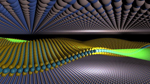
This particularly applies to materials called transition metal dichalcogenides (TMDCs). Previous research had shown that TMDC heterostructures have unusually large gaps between layers, which suggested that impurities might be trapped inside them.
The Manchester team built a heterostructure from two well studied TMDCs – molybdenum and tungsten diselenide – in an argon atmosphere in the closely controlled confines of a glove box, and then used high-resolution electron microscopy to investigate how the layers had stacked together.
“By taking a side view of these sandwich structures we can see how these unique materials stick together and discover new secrets we have previously missed,” said Aidan Rooney, who carried out the imaging.
In their paper, the team explains the flexibility in the thinnest TMDC flakes allows material to deform around impurities trapped between layers, which affects how the electrons from one layer interact with adjacent atoms.
In the same research, the team discovered that an air sensitive TMDC, niobium diselenide, can be assembled into pristine stacks in an inert atmosphere glovebox. This gives important insight into the best ways to manufacture such heterostructures to make the most of their potential properties, explained Dr Haigh.
“This sort of insight is changing how we build devices like LEDs and sensors from 2D materials. The properties of these devices were known to depend heavily on how and where we make them, and for the first time we have observed why.”


Project to investigate hybrid approach to titanium manufacturing
What is this a hybrid of? Superplastic forming tends to be performed slowly as otherwise the behaviour is the hot creep that typifies hot...