Since the discovery of graphene, engineers have become more familiar with the properties of ultra-thin, two-dimensional materials. But the potential applications for these materials have so far depended on the properties of only homogeneous stacks of these layers. Chemists and materials scientists at the University of California Los Angeles (UCLA) have developed a technique for forming “superlattices” consisting of layers of dissimilar materials. These substances could form the basis for superfast and ultra-efficient transistors in microprocessors, and advanced LEDs and lasers, they claim.
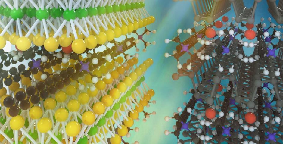
Artist's impression of, left, a molybdenum disulphide/ammonia superlattice, and right, black phosphorus/ammonia. Image: UCLA Samueli Engineering
The key to these tailored properties is that unlike current superlattices, where adjacent layers must have very similar atomic structures and therefore electronic properties, the new technique allows radically different structures, properties and functions to be placed next to each other, but without interfering with each other. For example, one layer could allow fast transport of electrons through or across it, while the next layer could be an insulator.
Described in Nature, the new superlattices alternate two-dimensional atomic crystal sheets with molecules of various shapes and sizes. The molecular layer is held in place by van der Waals forces, electrostatic attractions caused by asymmetry and fluctuating electron movement in the molecules, which are much weaker than the bonds between atoms in molecules or crystals. In effect, the molecular layer forms a second “sheet”.
"Traditional semiconductor superlattices can usually only be made from materials with highly similar lattice symmetry, normally with rather similar electronic structures," said Yu Huang, a professor of materials science and engineering at the UCLA Samueli School of Engineering, who conducted the research with team leader Xiangfeng Duan, professor of chemistry and biochemistry. "For the first time, we have created stable superlattice structures with radically different layers, yet nearly perfect atomic-molecular arrangements within each layer. This new class of superlattice structures has tailorable electronic properties for potential technological applications and further scientific studies."
The method of assembling the superlattice is novel. Rather than manually stacking them on top of each other, which risks breaking layers and is time-consuming, or using chemical vapour deposition to grow sheets on top of each other, which requires different conditions for each layer that could alter the properties of the first layers grown, the team used a process called electrochemical intercalation. A negative voltage is applied to a 2D material injecting electrons into its structure. These attract positively charged ammonium molecules into the space between atomic layers. The ammonium molecules automatically self-assemble into new layers between the crystalline 2D sheets. The ammonium molecules can be altered with the hydrogen molecules of normal NH3 replaced by organic groups of varying shapes, sizes and functionality, creating an intercalated layer with the properties required for the bulk superlattice.
“Think of a two-dimensional material as a stack of playing cards,” Duan said. “Then imagine that we can cause a large pile of nearby plastic beads to insert themselves, in perfect order, sandwiching between each card. That’s the analogous idea, but with a crystal of 2D material and ammonium molecules.”
The team first demonstrated the technique using black phosphorus as the base 2D material, and intercalated ammonium between the layered phosphorus sheets. With this proving successful, they created a new superlattices with modified ammonium.


Swiss geoengineering start-up targets methane removal
Several rather dubious statistics in this report. IF methane had 120× the thermal effect of CO2 that would be TWO orders of magnitude. Two is not...