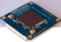
One problem with such devices, however, is that because each pixel on the imager has its own set of logic associated with it, the fill factor - or the percentage area that can be used to capture electrons - can never be 100 per cent if it is illuminated from the front, unlike a CCD sensor that can achieve close to a 100 per cent fill. This problem can be overcome if the sensor is illuminated from the back
To address that particular issue, the developers have created a second class of detector that sports an entirely different architecture. In these so-called double-sided strip detectors (DSSDs), silicon strips are fabricated on both sides of a detector to provide a means of pinpointing the exact coordinates of any electrons that pass through it.
’Unlike CCDs, and APS detectors - which fall into a class of sensor called integrating detectors - the DSSDs are counting detectors that can determine the position of an incoming electron from the charge that accumulates on strips that lie orthogonally on both the front and the back of the sensor as the electron passes though them,’ said Kirkland.
If a fast electron should land between two of the silicon strips on the front of the device, it will generate a signal in both, with the result that it is then impossible to determine the exact location of the electron. However, the signals created by such electrons can then be rejected by analysing the readout from the device using software, eliminating any potential errors and ensuring the accuracy of the device.
’One advantage such devices have is that their modulation transfer function - a specification that incorporates both resolution and contrast data - is almost perfect. Another is that, because they are counting the electrons that hit them, they have an absolute ability to measure the differences between light and dark while never becoming saturated,’ said Kirkland.
“One advantage of DSSD devices is that their modulationtransfer function is almost perfect”
PROF ANGUS KIRKLAND
The disadvantage of the DSSD devices is that, unlike APS devices, they do not incorporate arrays of picture elements that can be read out individually, so they can only capture images at several frames per second. While that might be somewhat faster than a CCD, it is nowhere near the thousands of frames per second which can be captured with the CMOS APS devices.
Although each class of sensors has its own set of advantages and disadvantages, Kirkland said that there is no reason why both the APS and the DSSD sensors could not play an equally important role in capturing images directly from next-generation transmission electron microscopes.
’We anticipate that such microscopes will eventually have two sensors - one sitting above the other - which you can move in or out of the electron optical column. The fast programmable APS sensor will be used for real-time viewing of dynamic events. When you want the ultimate resolution, you will remove the APS sensor, insert the DSSD and use that effectively as a digital film,’ he said.
At the present time Kirkland said that several prototype APS devices have been fabricated and the first electron beam tests of those devices should take place over the next couple of months.
As for the DSSDs, work is somewhat less advanced, although several small prototypes have also been fabricated. Later this year Kirkland plans to make some larger-scale DSSDs and use those to record image data.
design essentials
The key facts to take away from this article
- CCDs are currently used to capture images from electron microscopes
- This can result in images with losses or that have a limited resolution
- APS and DSSDs could help to obtain more accurate images
- Researchers say both could be used to capture images in the future


Swiss geoengineering start-up targets methane removal
No mention whatsoever about the effect of increased methane levels/iron chloride in the ocean on the pH and chemical properties of the ocean - are we...