Back-contact perovskite solar cells target greater efficiency
Solar cells could become more efficient and cheaper to mass produce as a result of an EPSRC-funded research project at St Andrew’s University.

The project, led by research fellow Dr Jonathon Harwell of the university’s physics and astronomy department, aims to develop a back-contact perovskite cell, improving efficiency and making the cells easier to mass produce.
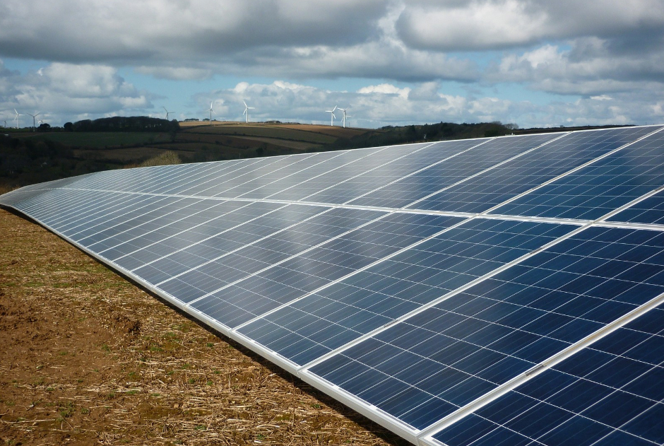
Perovskite describes a type of crystal structure, but in solar cells refers specifically to lead-halide perovskite, which is attracting intense interest because it has electrical properties like silicon. But whereas silicon must be grown slowly as crystals at temperatures of over 1000oC, perovskite is cheap to produce. It can be crystallised out of a solution of two inexpensive raw materials and deposited by methods including printing.
Perovskite solar cells have new potential thanks to materials study
Printed perovskite solar cell shows industry appeal
As a result, PSCs have the potential to be flexible, thinner and cheaper than silicon solar cells, with similar efficiency and with a lower cost of manufacture.
Register now to continue reading
Thanks for visiting The Engineer. You’ve now reached your monthly limit of news stories. Register for free to unlock unlimited access to all of our news coverage, as well as premium content including opinion, in-depth features and special reports.
Benefits of registering
-
In-depth insights and coverage of key emerging trends
-
Unrestricted access to special reports throughout the year
-
Daily technology news delivered straight to your inbox


UK Enters ‘Golden Age of Nuclear’
Anybody know why it takes from 2025 to mid 2030's to build a factory-made SMR, by RR? Ten years... has there been no demonstrator either? Do RR...