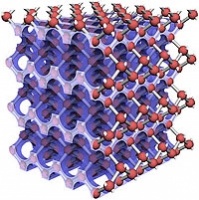
Intricate 3D silicon crystals act as semiconductors for light
Dutch researchers have found a way to make large silicon crystals with a true three-dimensional internal architecture.
This substrate platform could be used in both faster conventional complementary metal-oxide semiconductor (CMOS) electronics, as well as the emerging field of optoelectronics.
The computer industry is currently awaiting the next generation of microprocessors, which are likely to incorporate 3D elements, with so-called ‘fin’ structures.
By increasing surface area, they will be more conductive and powerful and also consume less power compared with conventional ‘planar’ chips. However, these chips are not inherently 3D, but rather comprised of stacked layers of separate chips.
Researchers at the University of Twente have now developed a method for making true 3D structures out of silicon. First they etch millions of tiny holes, 300 nanometres in diameter and around eight micrometres in depth, into the upper surface of a wafer of silicon, then tilt it and repeat the etching process.
In order to obtain the required architecture throughout, the second step has to be aligned extremely accurately relative to the first, with a maximum permissible deviation of just 30 nanometres and half a degree.
Register now to continue reading
Thanks for visiting The Engineer. You’ve now reached your monthly limit of news stories. Register for free to unlock unlimited access to all of our news coverage, as well as premium content including opinion, in-depth features and special reports.
Benefits of registering
-
In-depth insights and coverage of key emerging trends
-
Unrestricted access to special reports throughout the year
-
Daily technology news delivered straight to your inbox


UK Enters ‘Golden Age of Nuclear’
The delay (nearly 8 years) in getting approval for the Rolls-Royce SMR is most worrying. Signifies a torpid and expensive system that is quite onerous...