Richard Anslow, System Applications Engineer and Ricardo Zaplana, Design Engineer, both at Analog Devices
MEMS systems are used for vibration monitoring in railway, wind turbine, motor control, and machine tool applications to enhance safety, reduce costs, and maximise the useful life of equipment. MEMS sensors, with superior low frequency performance, enable earlier detection of bearing defects in railway and wind turbine applications compared to competing technologies. Significant cost savings are coupled with higher detection rates for equipment defects, ensuring compliance with stringent safety standards. Wide bandwidth (0Hz to 23kHz), low noise performance, and wide vibration measurement range (2g to 200g) are all required for vibration monitoring. This is easily achieved using Analog Devices’ broad MEMS portfolio.
Wired communication systems are used for vibration monitoring where raw data from several sensors is gathered, or where raw data is used for real-time control. There are several challenges in implementing a wired condition-based monitoring (CbM) system. One key challenge is electromagnetic compatibility (EMC) robustness when operating over meters of cabling, which can be subjected to indirect lightning surges, electrostatic discharges, and environmental noise such as switching of inductive or capacitive loads. Poor robustness to EMC disturbances can intermittently or permanently degrade the quality of data gathered from the CbM systems, as shown in Figure 1. Over time, poor quality data can lead to incorrect decisions around asset health and maintenance.
This article outlines key challenges in designing for EMC standards compliance with today’s highly integrated CbM solutions. Design for EMC is notoriously difficult to get right the first time, with even small changes in circuits or lab test setup dramatically affecting test results. This article presents a system-level EMC simulation approach or virtual lab, which helps the engineer to get the design EMC compliant in record time.

Figure 1. Wired CbM system with vibration sensors located in EMC harsh industrial environments.
Why Is System-Level EMC Simulation Important?
Modern product development schedules include a parallel EMC compliance task. Design for EMC should be as seamless as possible, but this is often not the case, with EMC problems and lab testing delaying product release by months. The virtual lab EMC simulation approach helps the engineer solve EMC problems much faster compared to lab test alone. The virtual lab simulation approach helps to solve key problems in achieving EMC compliance because:
- Increased integration and component density in modern PCB designs leads to complex problems, with multiple EMC failure Simulation can help to determine the best EMC mitigation technique, in a more flexible and time efficient way compared to lab testing alone.
- EMC standards are sometimes ambiguous, which means different test results are achieved if the circuit is tested in different Using simulation allows much faster test changes and results compared to lab testing.
- The entire system needs to be built to ensure EMC compliance, including cable choice, length, and shielding, as well as measurement Using simulation, real measurement probe effects can be ignored, and cable models can be changed in seconds rather than in hours.
- The equipment under test can differ from the customer’s installation, leading to different test Using simulation, the real customer application can be better modelled and understood.
- Existing simulation tools are not unified, and simulation models are not readily available for cables and PCB The virtual lab allows integration of cable, PCB, and passive and active component models, with more accurate results.
What Are the Benefits of System-Level EMC Simulation?
System-level EMC simulation results in much faster time to market for products. This is achieved through:
- Rapid identification of circuit weaknesses and targeted recommendations for improvement.
- 99% improvement in capturing EMC failures, and understanding the failure
- Significant cost savings - several design and test iterations do not need to be performed.
- Significant time savings - the design does not need to be iterated several times, which cuts down the development schedule by months when you consider the lead time for PCB board layout, manufacture, and assembly.
The EMC Challenge
Several EMC challenges are common in today’s highly integrated sensor system designs. Firstly, modern high density PCB design makes passing EMC tests a difficult task. Shared power and data wire architectures (phantom power) are often used to reduce system cost and PCB area (fewer PCB connectors). The IEPE standard, widely used with vibration sensor technology, supplies a constant current source to the vibration sensor, with the sensor output voltage read back on the same wire, as shown in Figure 2. This 2-wire system means that power supply and data communication lines are subject to the same EMC disturbance, adding additional complexity when designing for EMC. EMC filtering components need to be carefully chosen to mitigate against power supply disturbances, but also must not reduce the data circuit communication bandwidth.

Figure 2. A 2-wire IEPE sensor interface with shared data and power architecture.
Secondly, system-level EMC standards, such as IEC 61000-4-6 conducted RF immunity, are specified for many industrial products, with manufacturers stating product immunity to Class A (no communication errors) or Class B (communication errors, but the system does not need to be reset). The threshold for Class A compliance can vary from manufacturer to manufacturer and is usually identified by a bit error rate (BER), or equivalent microvolt or micro-g range for vibration sensors. The Class A compliance threshold is typically a very low voltage, much lower than the minimum signal that the system can measure. The conducted RF immunity standard allows the user to define pass/fail criteria for the system using a BER, while specifying some setup details and noise injection levels. There is plenty of scope for interpretation in regards to what is the most appropriate setup and BER, and this poses a challenge for the system designer: how to match the lab design verification test setup to the real customer application, particularly when small changes in test setup can yield dramatic changes in test results.
And thirdly, most common EMC test procedures need the full system to be built before going to the EMC certification lab to test it. Full systems include cable choice, length, and shielding. Different cables have different capacitance specifications, which in turn can couple more or less EMC noise into the affected system. Cable length and shield grounding can lead to impedance mismatches at high EMC frequencies as well as different ground current return paths. When a system is built, the preferred test method is that each sub-unit be individually tested for EMC immunity; however, in the real application the entire system will be subjected to the same EMC noise. These are just some of the reasons why it is difficult to correlate factory EMC testing with customer lab tests.
Given today’s highly integrated designs and EMC test complexity, it is clear that a time efficient flexible approach to design for EMC is needed. Simulation before and during lab testing is the answer. Getting the right lab results, with minimum time and effort invested, is the goal.
Using Virtual Lab to Accelerate Debug and Solve EMC Issues
Analog Devices’ system-level expertise and EMC simulation techniques have resulted in the development of a virtual lab simulation flow, as described in Figure 3. A virtual lab environment makes it easier to get design for EMC right the first time, with virtual design iterations performed instead of time-consuming and costly lab setup and measurement iterations. Computing power, SPICE, electromagnetic field simulators, and CAD software have converged and reached a maturity point where this virtual lab is feasible, where engineers can now achieve unprecedented levels of accuracy and simulation speed. PCBs, cables, integrated circuit chips, and passive components can be modelled, as well as EMC stimulus. The results can be analysed, with rapid identification of circuit weaknesses and targeted recommendations for improvement.
Using the virtual lab environment, the designer can access any physical node of the system during the tests without the typical measurement limitations found at the real lab - for example, measurement equipment bandwidth, lab limitations, non-ideal impedances of the probes, and external noise - interfering with the measurements.

Figure 3. Moving from the real lab to virtual lab environment.
Several common industrial IEC 61000 system-level EMC standards tests can be simulated prior to PCB fabrication, as detailed in Table 1.
Table 1. Simulation of Common IEC 61000 Industrial System-Level EMC Standards

MEMS and Simulation Case Study
This section describes a simulation case study and correlation with lab measurements, using the Figure 4 vibration monitoring circuit with Analog Devices’ ADXL1002 MEMS accelerometer. The circuit is compatible with the widely used IEPE interface, as described in Figure 2. The circuit contains two shunt regulators, one of which (IC1) powers the accelerometer and the AD8541 op amp (IC3), and a second (IC4) that provides a 9.5V dc bias. When the system is powered and the ADXL1002 is static, the communication bus rests at 12V dc. The circuit in Figure 3 requires compliance to IEC 61000-4-6 conducted RF immunity, which is a common requirement for equipment operating in industrial applications.
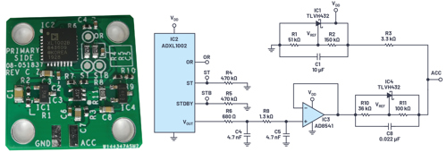
Figure 4. MEMS circuit using ADXL1002 and IEPE-compatible interface.
Correlating real lab and virtual lab simulation requires several process steps, summarized as follows:
1. Real lab setup and simulation environment correlation
2. Develop simulation models using virtual lab (Figure 3)
3. Use simulation to identify design for EMC weaknesses
4. Use simulation to identify design for EMC improvements
5. Validate design for EMC improvements in the real lab
Step 1: Real Lab Setup and Simulation Environment Correlation
The IEC 61000-4-6 conducted RF immunity test is applicable to products that operate in environments where radio frequency (RF) fields are present. The RF fields can act on the entire length of cables connected to installed equipment. In the IEC 61000-4-6 test, an RF voltage is stepped from 150kHz to 80MHz. The RF voltage is 80% amplitude modulated (AM) by a 1kHz sinusoidal wave. The IEC 61000-4-6 standard specifies Level 3 as the highest RF voltage at 10V/m. The RF voltage is injected to the cable shield, or capacitively coupled using a clamp.
As shown in Table 2, several key parameters need to be correlated between the virtual and real lab environment:
- Test level and IEC EMC standard (amplitude, frequency)
- Cable specification (length, capacitance, shielding)
- System grounding (including cable shield)
- Measured parameters (what and where in the circuit)
- Test pass/fail threshold (amplitude, frequency)
Table 2. Real Lab Setup and Simulation Environment Correlation

Step 2: Develop Simulation Models Using Virtual Lab
Typically, SPICE models are readily available for most active and passive circuit components. Electromagnetic simulators can model other nonstandard components, such as PCB geometry and nets, as well as cable models.
The information gathered in Table 2 helps to ensure accurate modelling of cable parameters. This system uses a 2-core shielded cable, which comes at a cost premium compared to an unshielded cable. Having no cable shield makes the system weaker from an EMC point of view. Simulation with an unshielded cable shows significant additional EMC noise compared to a shielded cable system.
The MEMS IEPE circuit, shown in Figure 4, is designed to be as compact as possible (1.9cm × 1.9cm) and uses just two PCB layers. Using a 2-layer PCB increases potential EMC issues due to higher coupling capacitances and crosstalk, so careful design is a must.
At this point, the system design engineer can start extracting the models for the PCB and cables, using electromagnetic simulation tools, and link those to the SPICE models of the ICs and passive components. Now a SPICE simulation can be performed, and EMC stimulus can interact at the system level. Figure 5 shows the electromagnetic simulation model for the PCB physical geometry and nets, and the 2-core shielded cable. The 3-dimensional PCB SPICE model is a complete abstraction of the PCB physical layout. The 3D PCB SPICE model includes many pins that can be used to connect to the MEMS, op amp, and shunt regulator SPICE models. In this way, an extremely accurate electrical simulation can be performed. Passive component values (capacitor, resistor, inductors) can be changed, and the system resonances can be observed and rectified in a more time efficient and flexible manner compared to changing and testing real hardware. The cable SPICE model can be modified during testing - for example, the cable length can be increased or decreased, which can have a significant effect on EMC coupling and system performance.
Once the EMC time domain simulation is finished, engineers can analyse the circuit transient responses across time and frequency. Depending on the type of EMC test, transient or frequency analysis must be done. Examples of transient analysis can be conducted immunity tests, and examples of frequency domain are radiated emissions EMC tests (see Table 1 for more information).

Figure 5. Electromagnetic simulation model for the PCB physical geometry and nets, as well as the 2-core shielded cable.
Step 3: Use Simulation to Identify Design for EMC Weaknesses
The failure mechanisms were easy to find once the full system was modelled and simulated. The EMC noise voltage is injected into the cable shield. The noise voltage is then coupled through parasitic capacitance between cable shield and wire cores. The noise is directed toward the ACC node on the PCB, as shown in Figure 6. The noise current path follows the path of least impedance, in this case through capacitor C8 to the op amp output. The op amp saturates as a result, sinking high current out of the power supply (VDD) node. The IC1 VDD regulator cannot supply this high current; therefore, the VDD voltage drops. The VDD voltage drop temporarily shuts down the MEMS sensor (powered at 5V nominal), resulting in voltage ripple at op amp output (noise).

Figure 6. Circuit failure mechanism.
A second failure mode was identified, which would be either difficult or impossible to observe and debug using lab testing alone. High frequency transmission lines are usually terminated with a load that matches the transmission cable impedance. The IEPE cable is typically unterminated due to low frequency (kilohertz) data communication. However, when the EMC noise is injected in the 60MHz to 70MHz range, noise voltages are reflected on the communication bus as the cable is not terminated with a matching load.
Step 4: Use Simulation to Identify Design for EMC Improvements
The goal is to determine the least costly and most effective circuit changes for EMC mitigation. The two EMC issues can be resolved by adding two capacitors, as shown in Figure 7. The 22nF CEMC directs the noise away from the sensitive circuitry (op amp, MEMS), with the noise current now shunted to ground via the C1 capacitor as shown. A ferrite bead, with high impedance at 100MHz frequencies, can be added for extra insurance to block any residual noise. The CTERM shunts cable reflections at high frequency during EMC testing.

Figure 7. Design for EMC improvements.
As described in Step 3, the VDD power net failure is a reliable indicator of EMC susceptibility. Figure 8 shows the voltage drop in the VDD power net where the CEMC is not used. The simulation predicts approximately 2V drop, or larger. When CEMC is used, the deviation from nominal is in the microvolt range, which is much lower than the target compliance threshold of 1.6mV.

Figure 8. Simulated VDD power net with CEMC capacitor (green waveforms) and without CEMC (blue waveforms).
Analog Devices’ ADXL1002 MEMS sensor has a 3db bandwidth of 11kHz, so the selection of the CEMC and CTERM is critical in order to preserve the 11kHz communication bus. Using the virtual lab flexibility, many capacitance values were simulated, and two optimum capacitance values were selected. After adding these capacitors, the system is predicted to meet the EMC pass criteria of less than 1.6mV of noise voltage.
Step 5: Validate Design for EMC Improvements in the Real Lab
The original circuit, as described in Figure 4, was lab tested using the Table 2 parameters. The result was a gross failure of 912mV of noise at a 77MHz test frequency.
Following the Step 4 recommendations, a 22nF capacitor (CEMC) was added in parallel with resistor R3. This resulted in a 99% improvement, with less than 6mV noise measured, as shown in the Figure 9 lab test result (blue waveform).
To achieve the design target of less than 1.6mV of noise, a 100nF CTERM was added between the ACC and GND nodes, as well as the CEMC 22nF. Figure 9 shows the green simulation result with the noise curve flattened across the broad 0.15MHz to 80MHz spectrum.

Figure 9. Simulation and lab test results following virtual lab recommendations.
Once the results and targets are achieved, it is possible to determine which part of the system is the weakest link from an EMC point of view. In this case, the cable is the main contributor as it couples the EMC energy from the source to the circuit and causes reflections due to its length and termination impedance at higher frequencies. The two capacitors (CTERM and CEMC) were able to shunt the two noise sources to the cable to ground effectively. Alternative solutions and approaches, such as it replacing the op amp, are unrealistic. Replacing the op amp with an ultralow output impedance op amp is a poor choice, as lower output impedance devices have inherently higher power consumption, which affects the competitiveness of the overall design.
Conclusion
Simulating the entire system gives unprecedented insights into how the circuit behaves under EMC stress and is the best way to solve complex EMC problems. Time to market can be dramatically reduced when this methodology is used. Greater than 99% improvement in design for EMC was achieved using the process flow described in this article, which is summarised in Figure 10.

Figure 10. Process flow for greater than 99% improvement in EMC performance.
About the Author
Richard Anslow is a system applications engineer with the Connected Motion and Robotics Team within the Automation and Energy Business Unit at Analog Devices. His areas of expertise are condition-based monitoring and industrial communication design. He received his B.Eng. and M.Eng. degrees from the University of Limerick, Limerick, Ireland. He can be reached at richard.anslow@analog.com.
Ricardo Zaplana holds a master’s degree in telecommunications and microelectronics from Universidad de Valencia, Spain. He has over 20 years of microelectronic design experience in areas of power management, interface, and isolation products. Ricardo now focuses on high speed isolators, isolated power, and EMC simulation, in the area of radiated emissions and conducted immunity. He can be reached at ricardo.zaplana@analog.com.


Water Sector Talent Exodus Could Cripple The Sector
Well let´s do a little experiment. My last (10.4.25) half-yearly water/waste water bill from Severn Trent was £98.29. How much does not-for-profit Dŵr...