
Industrial and medical design continually push to improve product accuracy and speed. The analogue integrated circuit industry has generally keptup with speed requirements, but it is falling behind on accuracy demands. There is a march toward 1ppm accurate systems, especially now that 1ppm linear ADCs are becoming common. This article presents op amp accuracy limitations and how to choose the few op amps that have a chance of 1ppm accuracy. We will also discuss a few application improvements to existing op amp limitations.
Accuracy is about numbers: how closely a system works to intended numerical value. Precision is about the depth of the numerical value in terms of digits. In this article we will use accuracy as a term that includes all limitations to system measurements, such as noise, offset, gain error, and non linearity. Many op amps have some error terms at ppm levels, but none have all the errors at the ppm level. For instance, chopper amplifiers can provide ppm-level offset voltages, dc linearity, and low frequency noise, but they have problematic input bias currents and linearity at frequency.Bipolar amplifiers can provide low wideband noise and good linearity, but their input currents can still cause in-circuit errors (we will hence use the term application for in-circuit). MOS amplifiers have excellent bias currents but are generally deficient in the low frequency noise and linearity areas.
In this article we will use the rough equivalency of 1ppm nonlinearity in the transfer function as –120dBc distortion in harmonic distortion.
Non-ppm Amplifier Types
Let’s discuss the types of amplifiers we reject as not highly linear. The least linearity is found in so-called video or line driver amplifiers. These are wideband amplifiers with terrible dc accuracies: offsets in the several millivolts and bias currents in the 1µA to 50µA range, and usually with poor 1/fnoise. Expected accuracies are 0.3% to 0.1% at dc, although the ac distortion can be from –55dBc to –90dBc (2000ppm to 30ppm linearity).
The next category is older classic op amp designs, such as OP-07, that may have high gain, CMRR, and PSRR, and good offsets and noise, but that cannot achieve better than –100dBc distortion, especially into a 1kΩ or heavier load.
Then there are the cheap amplifiers, new or old, that cannot best –100dBc when loaded more heavily than 10kΩ.
There is the audio amplifier class of op amps. They are fairly cheap, and their distortions can be very good. However, they are not designed for and do not offer good offsets nor good 1/f noise. They also cannot deliver distortion beyond perhaps 10kHz.
There are op amps meant to support MHz signals linearly. These are usually bipolar throughout and have large input bias currents and 1/f noise. This application space sees more like –80dBc to –100dBc performance, and ppm performance is not practical with these op amps.
Current feedback amplifiers also cannot support deep linearity nor even modest accuracy, no matter how wideband nor huge their slew rates may be. Their input stage has a mess of error sources, and they do not have much gain nor input nor supply rejections. Current feedback amplifiers also have a thermal drift that extends fine settling times greatly.
Then we have the modern general-purpose amplifiers. They typically have a 1mV offset and microvolts of 1/f noise. They support –100dBc distortion but usually not when heavily loaded.
Op Amp Error Sources
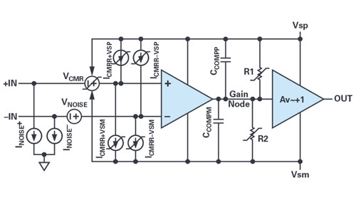
Figure 1 shows a simplified op amp block diagram with ac and dc error sources added. The topology is a single-pole amplifier with an input gmthat drives a gain node that is buffered as the output. While there are many op amp topologies, the error sources shown apply to them all.
Input Noises
We have an input noise voltage VNOISE with wideband and 1/f spectral content. You can’t measure a signal accurately if the noise is of similar magnitude or more than a system LSB. For example, if we had a 6nV/√Hz wideband noise and a 100kHz system bandwidth, we would have 1.9µVrms noise at the input. We could filter this noise down: for instance, dropping bandwidth to 1kHzdrops the noise to 0.19µVrms, or about 1µVp-p (peak-to-peak). Low-pass filtering in the frequency domain drops noise magnitude, as would averaging the output of an ADC over time.
However, 1/f noise cannot be practically filtered or averaged away because it is so slow. 1/f noise is usually characterized by peak-to-peak voltage noise generated in the 0.1Hz to 10Hz spectrum. Most op amps have between 1µVp-p and 6µVp-p low frequency noise and are thus not suitable for dc-accurate ppm levels, especially if providing gain.
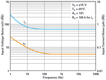
Figure 2 shows the current and voltage noise of a good high accuracy amplifier, the LT1468.
At the inputs in Figure 1, we also have bias current noise sources INOISE+ and INOISE–. They contain both wideband and 1/f spectral content. INOISE multiplies against application resistors to become more input voltage noise. Generally, the two current noises are uncorrelated and do not cancel with equal input resistors but add in rms fashion. Quite often INOISE times application resistors exceeds VNOISE in the 1/f region.
Input Common-Mode Rejection and Offset Errors
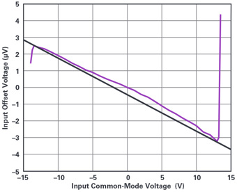
The next error source is VCMRR. This embodies the common-mode rejection ratio specification where an offset voltage changes inresponse to the input’s level relative to both supply rails (the so-called common-mode voltage, VCM). The symbol used indicates supply interaction at the arrows, and the segmented line through it suggests it’s variable but might not be linear. The major effect of CMRR on signals is that the linear part is indistinguishable from a gain error. The nonlinear part will be a distortion. Figure 3 shows the CMRR of an LT6018. The added line intersects extreme points of the CMRR curve just before the curve diverges into overload. The slope of the line gives a CMRR = 133dB. The CMRR curve diverges from a perfect line by only about 0.5µV per 30V span - a very successfully sub-ppm input. Other amplifiers can have much more curvature.
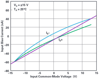
Offset voltage (VOS) will be lumped into CMRR here. Chopper amplifiers have sub-10µV input offsets, and that’s close to a single-ppm error, relative to typical signals of 2Vp-p to 10Vp-p. Even the best ADCs generally have as much as 100µV offset. So, the onus of offset is not so much on the op amps; the system will have to auto-zero itself, anyway. Associated with the input signal’s common-mode level is ICMRR, which is the input bias current and its variation with supplies. The broken lines suggest that the bias currents are variable with voltage and also may not be linear. There are four ICMRRs because both inputs can have independent bias currents and level dependencies, and because each input is varied by both supplies independently. The circuit effect of the ICMRRs(which sum to form bias current) is to multiply against application circuit resistances to add to overall circuit offset. Figure 4 shows the bias currents of an LT1468 vs. VCM (the ICMR specification). The slope as shown by the added line is ~8nA/V, which would be 8µV/V with a 1kμΩ applications resistor, or a low ppm error. The deviation from straight line is about 15nA, which in a 1kΩ application environment creates 15µV error over a 26V span, or a 0.6ppm nonlinearity.
Input Stage Distortion
Figure 1 shows the input stage, which is generally a transconductor made from a differential pair of transistors. The top of Figure 5 shows the collector, or drain currents, of various differential amplifier types vs. differential input voltage. We simulate a simple bipolar pair, a translinear circuit that we will call clever bipolar, a subthreshold (that is, very large) MOS differentialpair, a bipolar pair with emitter resistors (degenerated in Figure 5), and a smaller MOS pair operating out of the subthreshold region and into its square-law regime. All differential amplifiers are simulated with a 100μA tail current.
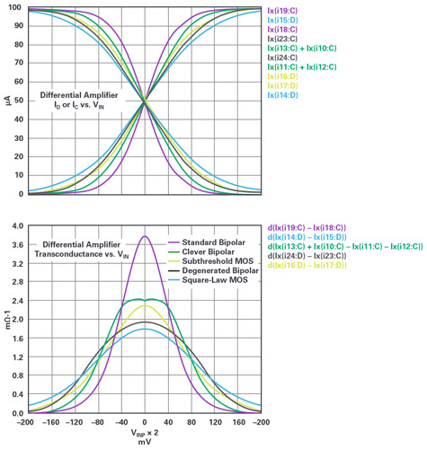
Not a lot of information is obvious until we display transconductance vs. VIN, as shown at the bottom of Figure 5. Transconductance (gm) is the derivative of output current with respect to the input voltage, as generated using the LTspice® simulator. The syntax has d() to be mathematically equal to d()/d(VINP). The non-flatness of gm is the basic distortion mechanism of op amps at frequency.
At dc, the open-loop voltage gain of the op amp is ~gm (R1||R2), assuming the output buffer gain is about unity. R1 and R2 represent the output impedances of various transistors in the signal path, each connected to a supply rail or other. This is thebasis of limited gain in an op amp. R1 and R2 are not guaranteed to be linear; they are a cause of unloaded distortion or nonlinearity. Aside from linearity, we need gains approaching or exceeding one million for ppm gain accuracies.
Observing the standard bipolar curve, we see it has the greatest transconductance of the group, but that transconductance fades quickly as the input moves from zero volts. This is concerning - a basic requirement for linearity is constant gain or gm. On the other hand, who cares that the amplifier voltage gain is so high that the differential input would only move microvolts as the output moves volts? Time to introduce CCOMP.
CCOMP (the parallel of CCOMPP and CCOMPM) absorbs most of the gm’s output current over frequency. It sets the gain bandwidth product (GBW) of the amplifier. GBW establishes that, at a frequency f, the amplifier will have an open-loop gain of GBW/f. Ifthe amplifier is outputting 1Vp-p at f = GBW/10 with a closed-loop gain of +1, then we have 100mVp-p between the inputs. That’s ±50mV from balance. Note that the standard bipolar curve shown in Figure 5 has lost about half its gain at ±50mV, guaranteeing massive distortion. However, the clever bipolar only lost 13% of its gain, the subthreshold MOS lost 26%, the degenerated bipolar lost 12%, and the square-law MOS lost 15%.
Figure 6 shows the distortion vs. amplitude for the input stage. This will appear (times the noise gain) at the output of the application circuit. You may get more output distortion than this, but not less.
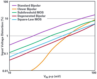
Excluding the clever bipolar stage, the differential amps show that the distortion is proportional to the square of the input. In a unity-gain application, the output distortion contribution is equal to the input distortion. This is the dominant distortion source for most op amps.
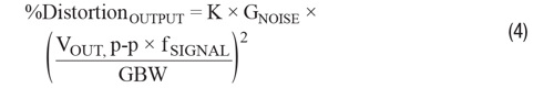
Consider a unity-gain buffer with a bipolar input. For an output of VOUT peak-to-peak volts, the input differential signal would be

We estimate that
And
where GNOISE is the noise gain of the application.
A 1ppm nonlinearity is like –120dBc harmonic distortion, and that’s 0.0001%. Given an amplifier with a bipolar input stage, a15MHz GBW, and outputting 5Vp-p as a buffer, Equation 2 tells us that the maximum frequency for that linearity is just 548Hz. This assumes the amplifier is at least that linear at lower frequencies. Of course, when the amplifier provides gain, the noise gain increases and the –120dBc frequency drops.
The subthreshold MOS input stage supports –120dBc up to 866Hz, square-law MOS up to 1342Hz, and degenerated bipolar up to 1500Hz. Clever bipolar does not follow the distortion prediction and one must get estimates from the data sheet.
We can use the simpler formula
where K is found from the distortion curves of an op amp’s data sheet.
As a side-note, there are many op amps with rail-to-rail input stages. Most get this ability from two separate input stages that have a hand-off from one to the other over the input common-mode range. This hand-off generates changes in offset voltage, and potentially bias current, noise, and even bandwidth. It also essentially causes a switching transient at the output. Theseamplifiers cannot be used for low distortion if the signal ever traverses the crossover region. An inverting application may work,however.
We haven’t discussed slew-enhanced amplifiers yet. These designs do not run out of current with large differential inputs. Unfortunately, small differential inputs still cause variations in gm of similar magnitude to the inputs discussed, and low distortion still demands a large loop gain at frequency.
Since we are looking for ppm-level distortion, we will not operate the amplifier anywhere near its slew rate limit, so, oddly enough slew rate is not an important parameter for ppm linearity at frequency, just GBW.
We’ve discussed open-loop gain as modeled by a single-pole compensation design. Not all op amps are compensated that way. Generally, open-loop gain is taken from the data sheet curve, and GBW/(GNOISE × fSIGNAL) in the equation is that open-loop gain at frequency.
Gain Node Errors
The next items in Figure 1 to discuss are R1 and R2. These resistors, along with the input gm, give the amplifier its open-loop dc gain of gm × (R1||R2). These resistors have been drawn with the variable and nonlinear strikethrough in the schematic. Nonlinearities of these resistors embody the amplifier’s unloaded distortions. Further, R1 injects influence from the positive supply such that the dc positive power supply rejection ratio (PSRR+) and is approximately equal to gm × R1. Similarly, R2 is responsible for PSRR–. Note how PSRR is almost equivalent to open-loop gain in magnitude. CCOMPP and CCOMPM have an analogous injection of supply signals to R1 and R2; they set PSRR+ and PSRR– over frequency.
It is possible that an amplifier with modest gain (<<106) can be quite linear, but that modest gain will limit gain accuracy.
The power supply terminals can be a source of distortion. When the output stage drives a heavy load, that load current flows fromone of the supplies. At frequency, the distant source of the supply may have little remote regulation, such that the op amp’s bypasscapacitors are the real supply source. The supply current drops across the bypass capacitors. These drops are dependent on theESR, ESL, and the reactance, and they cause a supply disturbance. Since the output is class AB, only half of the output currentwaveform modulates the supply, creating even harmonic distortion. PSRR over frequency attenuates the supply disturbance. As an example, if we observed 50mVp-p supply disturbance and wish the PSRR-induced input disturbance to be less than 5µVp-p, we need a PSRR of 80dB at signal frequency. Estimating that PSRR(f)~Avol(f), an amplifier with a 15MHz GBW would have enough PSRR at frequencies below 1500Hz.
Output Stage Distortions
The last item in Figure 1 is the output stage, which is considered a buffer for this discussion. A typical output stage transfer function is shown in Figure 7.
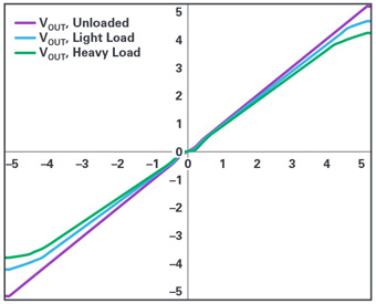
For the different loads, we see four kinds of error. The first is clipping: although this hypothetical output stage has a gain of 1 nominally, it’s not quite a rail-to-rail output stage. Even the unloaded output clips, in this case, 100mV from each supply rail. The output clips at successively lower voltages as the load is increased (decreased load resistance). Obviously, clipping is a disaster for distortion and the output swing must be reduced to avoid it.
The next error is gain compression, which we see as curvature in the transfer function at the extremes of signal. The compression happens at earlier voltages as the load is increased, and like clipping no ppm-level distortion is generally possible in this regime. This compression is generally due to a small output stage that is struggling to output required current. A good rule of thumb is that the linear, uncompressed maximum output current available from the amplifier is only about 35% of output short-circuit current.
Another glaring source of distortion is the crossover region around VIN = 0. Unloaded, the crossover kink may not be apparent, but with increasing loading we get something like the exaggerated kink of the green curve. Eliminating crossoverdistortion generally demands robust supply current.
The last distortion is harder to perceive. Because there are some bits of amplifier circuitry that output positive voltages and currents, and other bits for negative signals, there is no guarantee that they have the same gain, especially when loaded. Figure 7 shows a lesser gain for negative signals when loaded.
All these distortions are reduced by loop gain. If the output stage had 3% distortion, we would need a loop gain of 30,000 to get to a –120dBc level. That of course happens below a frequency of GBW/(30,000 × GNOISE), generally in the 1kHz regime for a 15MHz amplifier.
Some output stages’ distortions are frequency-dependent, but many are not. The open-loop gain suppresses the output stage distortion, but that gain falls with frequency. If the output distortion is constant with frequency, then the gain loss creates an output distortion that increases linearly with frequency. Meanwhile, input distortion causes a total output distortion that increases with frequency. In this case, the input distortion will probably dominate the total closed-loop output distortion, masking the output stage distortion contribution.
On the other hand, if the output stage distortion does vary, say, linearly with frequency, the falling loop gain creates anotheroutput distortion that varies as frequency squared, additional to and indistinguishable from input distortion.
Low power op amps generally have starved output stages whose quiescent currents are low. These amplifiers’ output stages may well dominate output distortion, rather than the input stage. It is somewhat true that it takes at least 2mA supply current to make a low distortion op amp.
Required Specifications for ppm-Level Accuracies
In practical level-shift, attenuate/gain, and active filter circuits, we have some basic op amp requirements for an amplifier supporting ±5V signal while working in a 1kΩ environment and achieving 1ppm linearity shown in Table 1.
Table 1. List of Op Amp Errors and Magnitude Needed for ppm Accuracy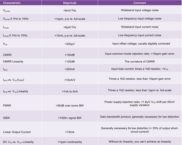
So, we see the limitations of op amps in the ppm accuracy world - can we do anything to improve them?
Noise: Obviously the first step is to select an op amp with input noise voltage no higher than an application resistors’ combined noise. One could reduce the overall impedance of applications circuits to reduce their noises. Of course, as the applications’ impedance drops, the signal currentsthrough them increase and can increase load-induced distortion. In any case, there’s no reason to reduce the output noise of an op amp stage much below the input noise of the stage it drives.
Current noise will multiply against application impedances as more voltage noise. MOS inputs are attractive in having very low current noise, but they often have more 1/f voltage noise than bipolar inputs. Bipolar inputs have pA/√Hz levels of current noise that make non-trivial applications noise, but the 1/f current content can produce applications voltage noise greater than the 1/f voltage noise of the amplifier. A general rule of thumb is that the application impedance should be less than VNOISE/INOISE of the amplifier to avoid IBIAS-dominated application noise. The lower the VNOISE of a bipolar amplifier, the higher the INOISE will be.
Helping Op Amps Achieve Best Performance
Reducing Input Errors
Aside from selecting an op amp with superior CMRR, designers can use op amps in inverting circuits rather than noninverting. In inverting circuits, the inputs hug ground or some reference and do not induce CMRR errors at all. Not all applications circuits can be made inverting, and often no negative power supply is available for the negative signal excursions. Figure 8 shows two-pole Sallen-Key filters in non-inverting and inverting realisations.
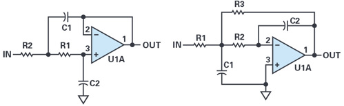
ICMR errors can be cancelled if both inputs have application resistors such that each input’s bias current gets cancelled as an output error by the appropriate resistances. For instance, if an amplifier is set up at a gain of 10 with 900Ω feedback and 100Ω ground resistors, placing a series 90Ω at the positive input will cancel perfectly equal bias currents at the output. The bias currents of most bipolar op amps are so well-matched that it is useful to choose 0.1% rather than common 1% resistors to achieve the best ICMR rejection. In Figure 8, the compensating resistors would be placed in series with each –input. They should probably be bypassed across. The extra input resistor contributes more noise, unfortunately.
Inverting gain allows us to use an op amp that has rail-to-rail inputs without the signal traversing a switching point - assuming we bias the supplies and common-mode input level to avoid that switching voltage.
Supply Considerations
Output currents will modulate the local supply voltage. That supply signal will find its way to the input through PSRR. The induced input will producean output signal that runs around its loop. At 1kHz, a 1μF local bypass capacitor has 159Ω of impedance, much less than the impedance of the line between the supply source plus that of the source itself. Thus, the local bypass capacitor won’t really be effective below 100kHz. At 1kHz, theremote supply controls regulation. At 1kHz the amplifier may have, say, 90dB supply rejection. Noting that most of the current from the op amp’ssupply terminals is made of even harmonics of the signal, we want the gain from the output to the offending supply to be lower than 30dB to make our120dBc goal. The gain of 30dB requires that the supply impedance should be <30× the load impedance. So, a 500Ω load requires a supply with lessthan 17Ω impedance. This is practical, but it does not allow a series isolating resistor or inductor between the supply and op amp. Things are tighter at10kHz; PSRR would drop from 90dB to 70dB, and the supply impedance would have to drop to 1.7Ω. Doable, but tight. A large local bypass would help.
From a layout point of view, it’s important to see where the output current loops go, as seen in Figure 9.
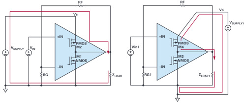
The diagram on the left of Figure 9 shows positive supply current driven into a load, coming from a supply, then returning through ground back to the load. There can be voltage drops all along the ground path, such that even-harmonic supply current drops voltage from the signal source to theoutput, and from the feedback divider to output or input ground. This ground is not that ground. The right side of Figure 9 shows a better way to route the supply currents. The supply current is dressed away from input and feedback nodes.
At higher frequencies, above 100kHz, the magnetic radiation of the supply lines can be a source of distortion. The even-harmonic currents of the supply can magnetically couple to the input or feedback network, dramatically increasing distortion with frequency. Careful layout is essential at these frequencies. Some amplifiers have nonstandard pinout; they keep the supply pins away from the inputs, and a few even offer an extra output terminal on the input side for to avoid magnetic interactions.
Reducing Load-Dominated Distortion
Many op amps’ output stages become dominant distortion sources when loaded heavily. There are a couple of tricks to improve loaded distortion. One is the composite amplifier: one amplifier drives the output and another amplifier controls it, as seen in Figure 10.
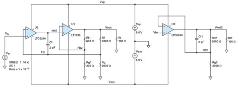
This from an LTspice simulation. The LTC6240 and LT1395 have macromodels that include distortion playback. Most macromodels do not attempt to display distortion, and even if they do the simulated value can be inaccurate. This writer was able to look at the text of the macromodels, and yes, in these macromodels distortion was modeled fairly well.
On the right of Figure 10 is an LTC6240 providing a gain of 2 while driving 100Ω - a difficult load for this amplifier. On the left of Figure 10 is a composite amplifier with another LTC6240 at the input, and a nice wideband current-feedback amplifier (CFA) to drive the same load as the standalone amplifier. The idea of the composite amplifier is that the output op amp already has a modestly low distortion, and that distortion can be reduced further by the input amplifier’s loop gain over frequency. We have the same closed-loop gain of 2 for both standalone and compositeamplifiers, but in the composite amplifier the LT1395 can be set up with its own gain (4 as set by Rf1 and Rg1) to reduce the output swing of the control amplifier. Since input-induced distortion increases as the square of output amplitude, there is a further reduction of distortion for the control opamp.
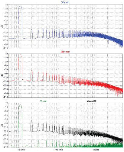
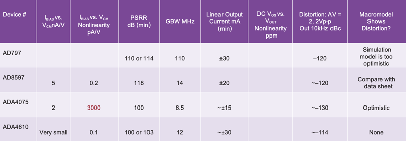
Figure 11 shows the spectrum of 10kHz, 4Vp-p outputs.
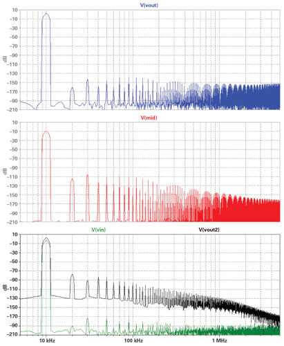
Harmonic distortion would be measured as each harmonic level (dB) minus the level of the fundamental (at 10kHz). As seen in the figure bottom the input signal has about –163dBc distortion, good enough to trust the simulation. V(out2) is from the unassisted LTC6240 and has –78dBc distortion. Not bad, but certainly not ppm-level.
The top of Figure 11 shows the composite amplifier distortion at –135dBc - pretty darn spectacular. Can we trust such a good result? For verification, the distortion at the schematic node mid is shown in the middle. If the output of a composite amplifier has near-zero distortion, but the output amplifier itself does have finite distortion, the feedback process will place the negative of the output amplifier’s distortion at its input (mid). Thedistortion at mid is –92dBc, and it actually matches the LT1395 data sheet curve! I would still wonder if the physical LTC6240 input CMRR or ICMR curvature is expressed in the macromodel - they may yet increase real circuit distortion.
Unfortunately, few macromodels include distortion. You’d have to read the header in macromodel .cir files to see if it is supported. Some simulation is required to see if distortion matches the data sheet curves.
Compensation of a composite amplifier can be a little tricky, but in our example, we have a second amplifier whose bandwidth is over 10 times that ofthe input amplifier’s, and just a little Cf compensates the circuit. In this compensation scheme, if the control amplifier has a bandwidth of BW at an overall gain, the output amplifier should have a bandwidth of >3 × BW, and the overall bandwidth will be conservatively set to ~BW/3.
To avoid losing bandwidth, we can use the boosted amplifier trick. It provides less distortion improvement than the composite approach but loses no bandwidth nor settling time. Figure 12 shows a test schematic.
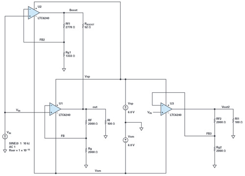
The right side of Figure 12 shows U2, our standalone LTC6240, and the left side shows two LTC6240 amplifiers. U1 controls the output and has again of two, like the standalone; U2 has a gain of three. U2’s output voltage at the boost node is larger than U1’s, so U2 drives current into theoutput. RBOOST and U2’s gain are configured such that U2 drives 96% of the load current into Rl, leaving a light load for U1 and thereby improving itsdistortion. One needs to assure that U2 has enough output headroom for its extra swing.
The LTC6240 has input-dominated distortion for loads in the kΩ range, but is output stage distortion dominated with our 100Ω load.
Figure 13 shows the spectral results.
Again, we have –78dBc distortion at 10kHz for the standalone amplifier. The boosted amplifier delivers –106dBc; not nearly as good as the composite amplifier, but almost 30dBc better than the standalone. However, the boosted amplifier suffers only a modest bandwidth reduction.
Note that RBOOST is tweaked; if we vary it as 52 ± 2Ω, the boosted distortion degrades by 10dBc, although little change thereafter happens for up to±10Ω. It would appear U1 likes to have some modest load of the expected polarity; ideal (no load) or excess boost current causes more distortion.
Ideally, U2 would have the same group delay as U1 so that the boost signal occurs at the same time as the output. U2 has 50% more gain than U1and thus has less closed-loop bandwidth, suggesting the boost output lags the main output at frequency. U1’s bandwidth could be reduced to be equal to U2’s by installing a resistor across U1’s inputs. This would increase the noise gain of U1 to be equal to U2 and achieve equality between the group delays. The simulator showed no improvement at 10kHz; U1 gave best distortion with no delay balancing. Knowing whether or not this is true at higher frequencies will require trying it. If the amplifiers were of current-feedback type, Rf1 and Rg1 could be reduced to bring U2’s bandwidth up to U1’s.
Recommended ppm-Quality Amplifiers
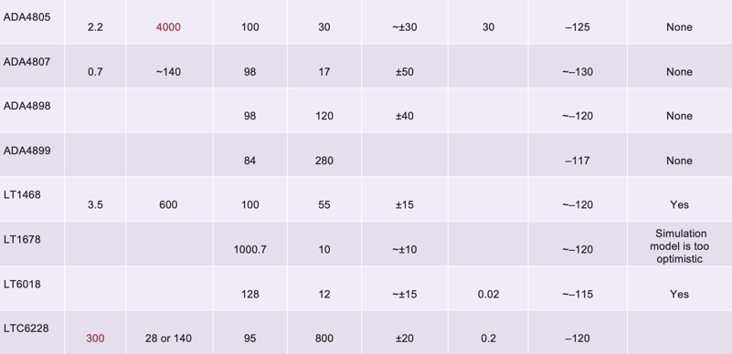
Table 2 shows the salient specifications for some suggested amplifiers approaching ppm linearity.
Entries are in red to alert the reader that a parameter may violate ppm-level distortion. The easy to use winners of the group are the AD8597, ADA4807, ADA4898, LT1468, LT1678, and LT6018.
There are some amplifiers that have input problems that must be dealt with (noninverting applications might be an issue) but that can still provide good distortion: AD797, ADA4075, ADA4610, ADA4805, ADA4899, and LTC6228.
Table 2. Salient Specifications for Some Suggested Amplifiers Approaching ppm Linearity
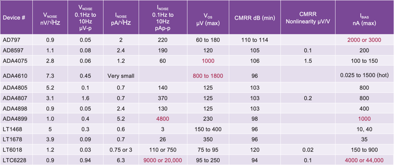
Table 3. Op Amp Comparison Continued
Conclusions
Sadly, commercially available ppm-accurate amplifiers are difficult, if not impossible, to find. There are ppm-linear amplifiers, but attention must be paid to the amplifier’s input currents that create distortion against application impedances. Those impedances can be lowered, but driving them in feedback runs the risk of creating distortion at the op amp input. By using an op amp with particularly low input currents and variations, the application impedance can be raised to obtain the best distortion from the op amp, but this will raise system noise. Careful op amp selection and applications circuitry optimisation are required for ppm linearity and noise.
About the Author
Barry Harvey has worked as an analogue IC designer, designing high speed op amps, voltage references, mixed-signal circuits, video circuits, DSL line drivers, DACs, sample-and-hold amplifiers, multipliers, and more. He has an M.S.E.E. from Stanford University. He holds more than 20 patents and has published about as many articles and papers. Barry’s hobbies include repairing used test equipment, playing guitar, and working on Arduino-related projects. He can be reached at barry.harvey@analog.com.


Water Sector Talent Exodus Could Cripple The Sector
Maybe if things are essential for the running of a country and we want to pay a fair price we should be running these utilities on a not for profit...