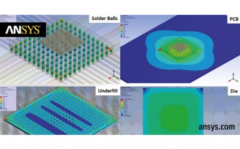
This paper presents a reference design flow for solving the electrical, thermal and mechanical challenges of a printed circuit board (PCB) using simulation tools from ANSYS. This approach can be utilized for all electrical CAD (ECAD) types such as IC packages, touch panel displays, and glass and silicon interposers. The authors followed this reference design flow for analyzing a PCB virtual prototype used in the consumer electronics industry. The design flow details nearly all aspects of the modeling technique from studying electrical connections in a schematic and setting up the PCB to analyzing the electrical, thermal and mechanical characteristics of the board — all using ANSYS tools. The multiphysics simulation yields power losses across the entire board and its objects, determines whether the integrated circuit (IC) and overall board temperatures lie within safe operating limits and predicts overall PCB reliability, taking into account all its components and heat sinks. Our reference design flow can help you solve multiphysics DC thermal and structural problems of any electronic product using ANSYS tools. You can do all of this analysis by using ANSYS products within a single framework wherein each product is tailored to solve a particular problem. By taking advantage of all the features and strengths of each ANSYS product, you can combine them to create a multiphysics solution for all the electrical, thermal and mechanical problems of a PCB.


UK Automotive Feeling The Pinch Of Skills Shortage
Aside from the main point (already well made by Nick Cole) I found this opinion piece a rather clunking read: • Slippery fish are quite easy to...