Introduction—Technology Innovations Will Lift the Last Hurdles to EV Mass Adoption
There are two major disruptions currently affecting the future of vehicular transport and semiconductor technology. The first is a shift from the internal combustion engine to the electric motor drive. The second is the emergence of new power switches (used in motor drive systems) that are based on wide band gap material. These offer figure of merit in the order of 10 times better than the incumbent solution based on silicon. However, with the battery accounting for more than 25% of the final vehicle cost, optimization of energy use is one of the keys to achieving mass electric vehicle (EV) adoption. Reaching this goal means recognizing that every watt spent is critical and prioritizing subsystem efficiency as the most important selection criteria in automotive system design.
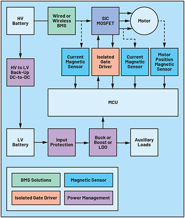
Recent advancements in power management for the powertrain (see Figure 1)—including isolated gate drivers, sensing, and BMS—provide opportunities for designers to be creative in order to improve system efficiency while keeping the system cost under control.
New Isolated Gate Driver Technology
Targeted for adoption by the next generation of traction inverters in the EV drivetrain, silicon carbide (SiC) MOSFETs—on their own merit—are widely expected to add between 4% and 10% more range for a standard EV driving cycle as compared to existing silicon-based technologies.1 Properly exploited with supporting componentry, this power efficiency gain could represent a huge step forward in building consumer confidence in EV range, and thereby help to accelerate EV adoption.
The first goal of the isolated gate driver is to protect persons and equipment from the high voltage present across the SiC switch. The second one is to ensure short and accurate propagation delay through the isolation barrier. Indeed, in leg configuration, as in traction inverter systems, there are two transistors (one high-side and one low-side), which should not be on at the same time to avoid short circuit. For this reason, the pulse-width modulation (PWM) signals coming from the microcontroller and going to the gates of the transistors need to have similar propagation delays. Then, as any delays need to be compensated, short propagation delay allows for the fastest control loop.
In addition to this, the isolated gate driver will take care of setting the best switching sweet spot, controlling power switch overheating, detecting and protecting against short-circuit, as well as facilitating the insertion of the sub-block drive/switch function in an ASIL D system.
All intrinsic advantages of the SiC switch would be negated by common noise perturbations as well as extremely high and destructive voltage overshoot due to ultrafast voltage and current transients generated in a poorly managed power switch environment. Broadly speaking, the SiC switch has a relatively simple function despite the underlying technology—it’s only a 3-terminal device—but it must be carefully interfaced to the systems.
Isolation: Key Element for System Efficiency
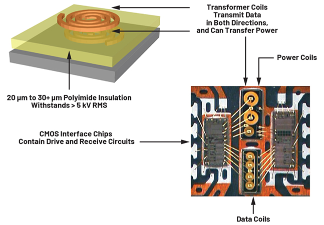
The high slew rate transients introduced by the SiC switch can corrupt data transmission across the isolation barrier, so measuring and understanding the system susceptibility to these transients are critical. Technology based on transformers with thick polyimide insulation (see Figure 2) exhibits ideal common-mode transient immunity (CMTI) with measured performances of up to 200 V/ns and beyond. Polyimide insulation technology unlocks the full potential of SiC switching time under safe operation.
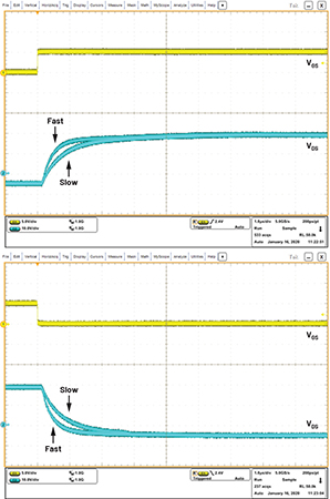
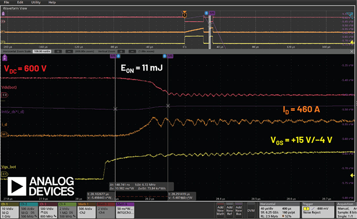
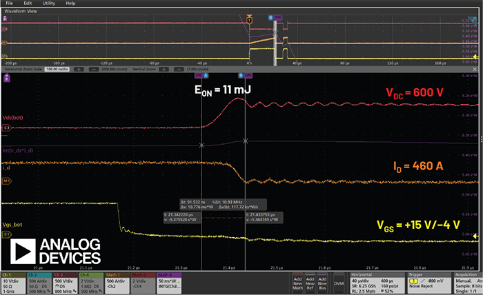
Switching energy and electromagnetic compatibility (EMC) can likewise be maximized to improve power performance and, ultimately, EV range. Higher drive capability allows designers to have faster edge rates and therefore reduces switching losses. Higher drive capability not only helps with efficiency but also enables board space and cost savings by eliminating the need for external buffers allocated per gate driver. Conversely, under certain conditions, the system may need to switch more slowly to achieve optimal efficiency, or even in stages that studies have shown can increase efficiency further. The ADuM4177 pre-released, 30 A gate driver provides top-of-the-range drive strength, adjustable slew rate (see Figure 3) and SPI. The device is rated for 1500 V peak and DC working voltage to DIN VDE V VD0884-11 and can be used either in 400 V or 800 V systems. Figures 4 and 5 show 11 mJ turn-on and turn-off switching energy at 600 V/460 A. One can also notice a minimal ringing at turn-on, as well as a very well-controlled overshoot at turn-off.
No Compromise with Robustness
Short circuits are a major obstacle for SiC-based power switches (MOSFETs), given the smaller die sizes and exacting thermal envelopes. Gate drivers provide the short-circuit protections essential for EV powertrain reliability, safety, and life cycle optimization.
High performance gate drivers have proven their value in real-world testing. Across key parameters including short-circuit detection time and total fault clearance time, performance can be achieved down to 300 ns and 800 ns, respectively. For additional safety and protection, test results have demonstrated the adjustable soft shutdown capabilities essential for smooth system operations.
Enter the Magnetoresistive (MR) Current Sensor Technology
As shown in Figure 1, DC and phase current need to be sensed for the inverter control loop. With a SiC power switch, a higher switching rate and switching frequency is possible, which can lead to higher efficiency and better regulation of the load when the control loop is given enough phase margin. To achieve a constant response and low phase delay at the switching frequency, the frequency of the current measurement needs to be at least a decade higher. This makes the bandwidth of a current sensing solution a key element in fully utilizing SiC switches.
Hall Sensor, a Hurdle to the Highest Performance
The traditional way of measuring current in traction inverters utilizes Hall sensors, which work by measuring the magnetic field generated by a current flowing through a conductor. However, their lack of sensitivity requires the use of a flux concentrator (or magnetic core) to amplify that magnetic field such that it can be measured. Modules combining a Hall sensor and a magnetic core are widely available but can lead to significant constraints on the system design. The modules are heavy, bulky, and prone to mechanical damage, which may become a reliability issue resulting in field returns. In addition, the presence of magnetic material in the core will have a strong impact on the frequency response, unless special and expensive material is used. Today the bandwidth of these modules is limited to 50 kHz to 100 kHz. This bandwidth limitation would require compromises to be made in the control loop, which will result in overall reduction in system performance.
The Challenges of Using a Shunt Solution
Another way of measuring lower current is through a shunt, a current sense amplifier, and an analog-to-digital converter (ADC). Shunts have been around for many years, continuously improving over time to achieve the stability they are known for. However, two major downsides of a shunt solution are self-heating (power dissipation being R×I²) and the need for isolation in certain applications. Self-heating may be reduced by decreasing the shunt resistance, but this will also reduce the amplitude of the signal of interest. Shunts also have a parasitic inductance, which limits the bandwidth of the current to be measured. With such limitations, power systems must look to a different technology to solve their current measurement challenge.
The Next Generation of Current Measurement and Simpler System Design: MR Sensors
MR sensors also work by measuring the magnetic field generated by a current flowing through a conductor. However, MR sensors can be significantly more sensitive than a Hall sensor, which removes the need for a magnetic core. Without this barrier, the inherent capabilities of the MR sensor itself, such as high bandwidth, accuracy, and low offset, allow for a simpler system design.
The removal of the bulky magnetic core means additional attention must be paid to crosstalk between phases and the possibility of external magnetic interference. Analog Devices’ solutions leverage the design flexibility of MR sensors to attenuate the effects of such interference. ADI offers design guides and tools to help engineers design a coreless current measurement system.
Coreless Sensing Using AMR Sensors
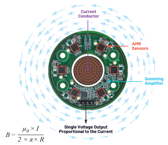
Figure 6 shows a solution that is not only higher bandwidth, more accurate, and lighter than a magnetic core-based solution, it is also built on a standard PCB, thereby reducing system complexity and integration cost. It presents a ring architecture consisting of six anisotropic magnetoresistive (AMR) sensors arranged in a circle to integrate the magnetic field to be measured. The integration of the magnetic field will reject external stray fields, enabling high rejection of a homogeneous stray field and low crosstalk. Each individual sensor senses the magnetic field generated by the wire/busbar placed in the center of the board. The outputs of these sensors are summed in the analog domain, and the resulting voltage output is directly proportional to the current flowing into the conductor.
The number of sensors used can be varied to achieve different levels of robustness to stray fields or to the tolerance of the wire placement within the ring. The diameter of the ring can be scaled up or down to match the targeted current range of the system. In this way, a single design approach—but with potentially multiple sizes—allows reuse across systems and platforms, enabling shorter development times and system cost reduction.
ADI will be releasing the ADAF1080 for the instrumentation and industrial market. With high magnetic range, inherently isolated measurement, and zero-offset over life and temperature leading to low output ripple and high efficiency in closed-loop systems, the ADAF1080 is paving the way to the next generation of current measurement. The ADAF1080 can achieve contactless and coreless current measurement, with a 3 dB bandwidth up to 2 MHz. Altogether these performances improve the inverter efficiency and in turn extend the vehicle range.
Power Management
On the road toward the highest performance, every watt matters whether the EV is in “on,” “standby,” or “sleep” mode. Cutting-edge power management solutions can further increase the overall vehicle efficiency, which correlates to extra miles while not compromising on the best EMC performance from low current/low voltage to high current/high voltage applications.
Design Challenges in High Voltage Flyback Circuits
In functionally safe systems, continuity of voltage supply is critical. The generation of a local low voltage rail from the high voltage battery plays a key role. In traditional isolated high voltage flyback converters, tight regulation is achieved using optocouplers to transfer regulation information from the secondary-side reference circuitry to the primary side. The problem is that optocouplers add significant complexity to isolated designs: there is propagation delay, aging, and gain variation, all of which complicate power supply loop compensation and can reduce reliability. Moreover, during startup, either a bleeder resistor or high voltage start-up circuit is required to initially power up the IC. Unless an additional high voltage MOSFET is added to the start-up components, the bleeder resistor is a source of unwelcome power loss.
No Need for an Optocoupler
By sampling the isolated output voltage from the third winding, no optocoupler is required for regulation. The output voltage is programmed with two external resistors and a third optional temperature compensation resistor. Boundary mode operation helps to achieve excellent load regulation. Because the output voltage is sensed when the secondary current is almost zero, no external load compensating resistors and capacitors are needed. As a result, the solution has a low component count, greatly simplifying the design of an isolated flyback converter.
Start-Up Optimization
With an internal depletion mode MOSFET (which has a negative threshold voltage and is normally on), there is no need for an external bleeder resistor or other start-up components. Once a local 12 V capacitor is charged, the depletion mode MOSFET turns off to reduce power loss.
Ultralow Quiescent Current
In order to achieve ultralow quiescent current, several mechanisms should be implemented. The switching frequency should be reduced at light load while keeping the minimum current limit in order to reduce current while properly sampling the output voltage. In standby mode, in implementing 16× reduction of its switching frequency (3.5 kHz to 220 kHz) as well as keeping the preload current at less than 0.1% of full output power, the LT8316 has demonstrated a quiescent current lower than 100 µA.
Extremely Wide Input Range Operation (18 V to 1000 V)
The LT8316 is rated to operate from a VIN of up to 600 V, but this can be extended by placing a Zener diode in series with the VIN pin in order to further improve the solution scalability. The voltage drop across the Zener diode reduces the voltage applied to the chip, allowing the supply voltage to exceed 600 V. With the 220 V Zener diode placed in series with the VIN pin, the minimum supply voltage for startup is 260 V, give or take, considering the voltage tolerance of the Zener diode. Note that after startup, the LT8316 will operate normally with a supply voltage below 260 V.
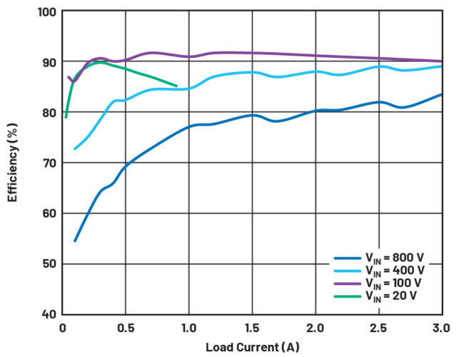
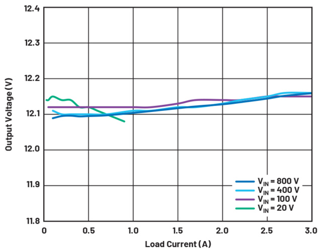
Figure 7 shows efficiency at various input voltages, with the flyback converter achieving 91% peak efficiency. Even with no optocoupler, load regulation at different input voltages remains tight, as shown in Figure 8.
Battery Management System
A BMS closely monitors and manages the state of charge (SOC) of a multicell battery string. For large, high voltage battery packs, such as those in an electric vehicle, accurate monitoring of each individual battery cell and the overall pack parameters are critical for achieving maximum usable capacity, while ensuring safe and reliable operation. The accuracy of the BMS will free up more energy from the battery, which directly translates to the miles per charge an electric vehicle can deliver, maximizes the battery’s overall lifetime, and as a result lowers the cost of ownership.
In 2009, Linear Technology (now part of ADI) brought the first cell monitor IC to the market. It integrated with op amps, muxes, and ADCs to measure cell voltage and temperature. More than 10 years later, with five generations of road-proven devices in more than 100 vehicle models, ADI is leading the BMS industry.
Lifetime Total Measurement Error (LTME)
Our most recent BMS product release is the ADBMS6815 (see Figure 9), which has an industry-leading 1.5 mV of LTME. That’s nearly 2× lower LTME relative to the industry benchmark.
Automotive OEMs and Tier 1s have confirmed each mV of LTME impacts the SOC estimation by upwards of 5%, requiring OEMs to be overly conservative when reporting the remaining range in the vehicle. For a high voltage pack worth
$9000, a 1% error in the SOC estimate can cost a system ~$90 per mV of error. LTME includes thermal hysteresis, solder reflow, quantization error (noise), sensitivity to humidity, and long-term drift.
In an 800 V system using 16 12-channel devices, a 4 mV error (state of the art) relative to ADBMS6815 with 1.5 mV error, has a ~$225 higher total cost of ownership, while enabling better SOC estimation and extending EV range.
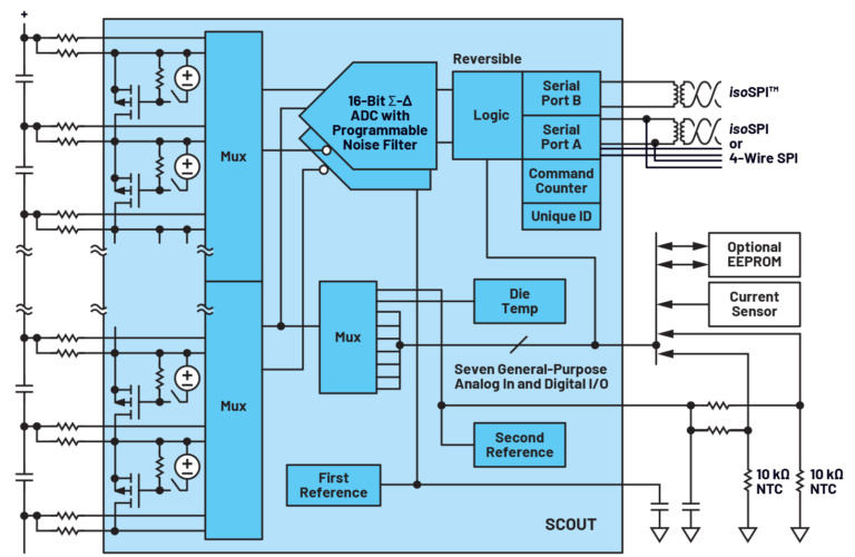
The ADBMS6815 has two 16-bit sigma-delta ADCs multiplexed across eight channels each, and comes with eight programmable oversampling ratios to allow filtering as low as 26 Hz and as high as 27 kHz. With 300 mA of cell balancing capability, the ADBMS6815 has eliminated the external discharge switches, saving ~$0.50 per BMS IC as well. Additionally, this device fully supports the newest requirements for giving an early warning of cell thermal issues by monitoring the cells even while the vehicle key is off.
Wireless BMS (wBMS)
A wBMS solution represents a combination of three technology pillars, namely BMS performance, radio solutions, and network protocol technology. A wBMS system solution is customized for automotive battery management use cases, delivering a safe, secure, robust, and scalable end-to-end wBMS system solution for next-generation EVs.
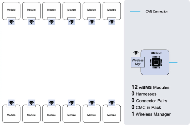
At the core of wBMS systems is the RF network. The network operates in the 2.4 GHz band and is a redundant star topology. This means each node in the network can communicate directly to 1 of 2 managers. The network also supports a 2-hop failover mode where, in case of a communication failure, a node can continue to communicate by hopping back to the network manager via another node. A wBMS system is a purpose-built network for battery pack and EV environments. The wireless system integrates a high performance 2.4 GHz radio with a time channel hopping MAC layer and a network layer that provides determinism as well as path, time, and frequency diversity. These key features combine to overcome the link and interference challenges in the operational environment.
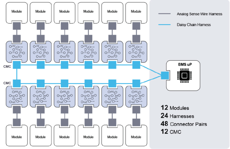
The elimination of the battery pack harness is one of the main characteristics that sets wBMS apart from BMS (see Figure 10 and Figure 11). Depending on the pack architecture, this can save up to 90% of the wiring and up to 15% of the volume in the battery pack systems for next-generation EVs, resulting in less pack materials and the possibility of higher (energy) density packs.
The removal of the battery pack communications harnesses also eliminates a hard constraint on the car design. This enables a modular pack system leading to simpler packs, automated/robotic assembly, and time and cost-efficient manufacturing processes. Simpler and more modular pack design opens the possibility of design reuse across a portfolio of EVs and results in a design flexibility that is unconstrained by accommodation of extensive harness and connector assemblies.
The wBMS Is a Key Enabler for a 2nd Life Battery Pack
To further improve the overall carbon balance of a vehicle, it is critical to think about battery pack second life. The battery pack should be closely monitored during its entire life cycle, and wBMS makes this easy to implement.
At the start of life, a battery module can spend long durations in transport or in warehouse inventory before pack assembly. Wireless BMS enables continuous open-circuit voltage and temp monitoring, which can identify early life failures before they become an issue. Additionally, lifetime traceability and monitoring can also be stored/updated continuously on standalone wireless enabled battery modules before pack assembly and throughout the battery life cycle. These features combined with the elimination of the communications harness enable an easier and cost-effective transition to the battery pack’s second life.
Conclusion
ADI’s powertrain innovative solutions, such as a new set of isolated gate drivers with over 150 V/ns CMTI protection and below 1 μs short-circuit protection, are unlocking the full potential of new SiC-based high performance traction inverter systems.
It’s important to note that the combined value and performance of the gate driver and SiC switch solution can be completely negated by compromises and/ or inefficiencies in the surrounding components. A system-level approach that encompasses a wide range of design considerations is key to performance optimization.
On the battery management side, ADI’s products address EV design challenges by offering superior battery sensing, the highest level of automotive safety, the broadest portfolio of EV BMS devices, and the most innovative, versatile system-level solutions.
Although the challenge for OEMs in adopting wBMS lies in planning for significant investments in design, validation, and manufacturing infrastructure, wBMS is projected to be much more cost-effective and otherwise advantageous in the long run, offering possibilities for increasing battery energy densities, improving design reuse and flexibility, and enabling extended features.
Authors:
Timothé Rossignol, Marketing Manager
Brian O’Mara, Automotive Program Manager
Kate O’Riordan, Applications Manager
Guilhem Azzano, Applications Engineer
Maurizio Granato, Strategic Marketing and Applications Manager
Sarven Ipek, Marketing Manager, and
Wei Gu, Applications Director


Comment: The UK is closer to deindustrialisation than reindustrialisation
"..have been years in the making" and are embedded in the actors - thus making it difficult for UK industry to move on and develop and apply...