
István Csomortáni, FPGA Design Engineer, Dragos Bogdan, Software Development Engineer Manager,
Cristian Orian, System Design Engineer, and Andrei Cozma, Engineer Manager, all with Analog Devices
Abstract
This article discusses Analog Devices’ new broad market LIDAR prototyping platform and how it helps shorten the customers’ product development time by providing a complete hardware and software solution that customers can use to prototype their algorithms and custom hardware solutions. It goes over the details of the modular hardware design, including the light receive and transmit signal chains, FPGA interface, and optics for long range sensing. The system partitioning decisions that were made are explained, helping highlight the importance of good system design, interface definition, and right level of modularity. The components of the open source LIDAR software stack and the platform specific API are described showing how customers can benefit from these during product development and integrate them in their final solutions.
Introduction
As autonomous vehicles and robots continue to move from science fiction to reality, automotive and industrial customers are seeking new environment perception solutions to enable these machines to navigate autonomously. LIDAR is one of the fastest growing technologies in this field and is seeing wider adoption as the technology becomes more mature and reliable, opening up a huge market opportunity. As many startups and well renowned sensor companies are working toward developing more precise, less power hungry, smaller form factor, and more cost-effective LIDAR sensors, they all face the same challenges when it comes to system hardware design and implementing the software infrastructure to talk to all the components in the system. These are the exact areas where ADI can bring value through hardware reference designs accompanied by open-source software stacks, enabling customers to easily integrate into their products ICs from the ADI LIDAR portfolio, as well as software modules and HDL IPs, shortening their time to market.
System Architecture
As customers develop their LIDAR sensors, there are few areas of differentiation in the system design: receive and transmit optics, number and orientation of lasers, laser firing patterns, laser beam steering, and number of light receive elements. But, regardless of these choices, there is a high degree of commonality in the receive signal chain and laser drive signal requirements. Based on these assumptions, Analog Devices designed a modular LIDAR prototyping platform, AD-FMCLIDAR1-EBZ, intended to allow customers to easily configure or replace parts of the design with their own hardware, designed according to specific applications requirements, but still be able to use the platform as a whole system. The system is partitioned into three different boards with standardized digital and analog interfaces:
- A data acquisition (DAQ) board containing a high speed JESD204B ADC and corresponding clocking and power. This board has an FMC compliant interface to connect to the users’ preferred FPGA development It serves as the baseboard in the system by having the other two boards connected to it via digital connectors that route control and feedback signals between these boards and the FPGA and through coaxial cables for analog signals.
- An analog front-end (AFE) board containing the avalanche photodetector (APD) light sensor and the entire signal chain required for conditioning the APD output signal so that it can be fed into the ADC on the DAQ
- A laser board containing the lasers and drive circuit.
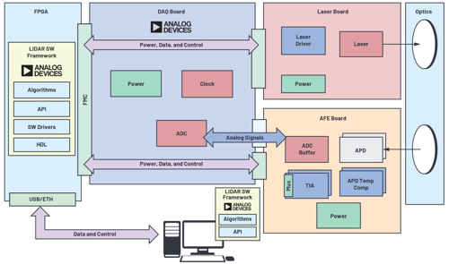
Figure 1. LIDAR platform system design.
As always, in system design, modularity means flexibility, but it also comes with drawbacks such as increased complexity, performance degradation, and increased cost, which must be thoroughly evaluated when deciding on the system partitioning. In this case, the system was broken down into these three boards for the following reasons:
- The ADC and clocking are very likely to stay the same regardless of the implementation of the analog front end and chosen laser solution.
- The analog front-end hardware design and form factor is subject to change depending on the chosen APD, overall system receive sensitivity, and chosen
- The laser board design and form factor are also subject to change depending on the chosen illumination solution and
- The system must provide a lot of flexibility in positioning and orienting the receiver and the transmitter so that they are aligned with each other or other targets, which is why flex cables are being used for the digital signals and coaxial cables for the analog signals that go between the
The software stack that accompanies the hardware design is based on a hierarchical approach with a few layers dividing it into OS specific drivers and interfaces, a system specific API, and an application layer. This allows the upper layers of the stack to remain unchanged regardless of whether the software is running on an embedded target or a PC talking to the system via the network or a USB connection. This is very valuable in the different product development stages, shown in Figure 2, since it means that the same application software that was developed during the prototyping stages, when the system is tethered to a PC for ease of development, can be easily deployed onto the embedded production system without ever touching the low level interfaces.
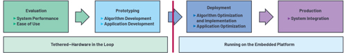
Figure 2. Product development cycle.
Hardware Design
A LIDAR sensor computes the distance to a target by measuring the time it takes for the light pulse to travel to the target and back. The time is measured in increments of the ADC sampling rate since that determines the resolution with which the system samples the received light pulse. Equation 1 shows how the distance is computed relative to the ADC sampling rate.

Where:
LS is the speed of light, 3 × 10⁸ m/s
fS is the ADC sampling rate
N is the number of ADC samples since the light pulse is generated until it is received back
Given the 1 GHz sampling rate of the AD9094 JESD204B quad ADC being used in the system, the results of each sample correspond to a distance of 15 cm. For this reason, it is critical that there aren’t any sampling uncertainties in the system since even an uncertainty of a few samples can result in large distance measurement errors. Traditionally, LIDAR systems are based on parallel ADCs that inherently provide zero sampling uncertainty. As the number of receive channels keeps increasing and the power and PCB size requirements become more stringent, these types of ADCs do not scale well. Another option is to use ADCs with high speed serial outputs, such as JESD204B, which solve the issues the parallel ADCs have. This option comes with an increased complexity on the data interface and makes it harder to achieve zero sampling uncertainty.
The LIDAR DAQ board provides a solution to these challenges by showing how to design the power, clocking, and data interface for a JESD204B data acquisition system operating in Subclass 1 mode, ensuring deterministic latency so that zero sampling uncertainty can be achieved, while taking advantage of all the benefits that the JESD204B interface provides and having the lowest possible power for the clocking scheme. To operate in JESD204B Subclass 1 mode, there is a total of five clocks needed in the system:
- ADC sampling clock: drives the ADC signal sampling process.
- ADC and FPGA SYSREF: source synchronous, high slew rate timing resolution signals responsible for resetting device clock dividers to ensure deterministic
- FPGA global clock (also referenced as core clock or device clock): drives the output of the JESD204B PHY layer and FPGA
- FPGA reference clock: generates the PHY layer internal clocks needed by the JESD204B transceivers; needs to be equal to or an integer multiple of the device
All the clocks are generated by one AD9528 JESD204B clock generator, thus ensuring they are all synchronized with each other. Figure 3 shows the clocking scheme and the data interface with the FPGA.

Figure 3. DAQ board clocking and data path.
The AFE board receives the optical reflected signal, converts it to an electrical signal, and transfers it to the ADC on the DAQ board. This board is probably the most sensitive part of the entire design since it mixes signal condition circuits working with microampere current signals generated by the 16-channel APD array, converting the optical signal to an electrical signal, with high voltage power supplies in the range of –120 V to –300 V needed to power the same APD. The 16 current outputs are fed into four low noise, four-channel, transimpedance amplifier (TIA) LTC6561s with an internal 4-to-1 mux to select the output channel that is afterward fed into one of the four ADC inputs. The input section of the TIAs needs a lot of attention to achieve the desired level of signal integrity and channel isolation so that there is no additional noise added to the very low current signal generated by the APD, thus maximizing the SNR and the object detection rate of the system. The design of the AFE board shows the best practices to achieve the maximum signal quality by keeping the length of the traces between the APD and the TIA as short as possible, adding vias in between the TIA inputs for maximum channel-to-channel isolation, and positioning the signal condition circuits so that they do not interfere with the other power circuits on the board. Another important feature is the ability to measure the temperature of the APD to be able to compensate for APD signal output variations due to temperature changes as the APD’s temperature increases during normal operation. A few knobs are provided to control the offsets of the signal chain and the APD bias, which translates into APD sensitivity, to be able to maximize the ADC input range for maximum SNR. Figure 4 shows a block diagram of the AFE board signal chain.
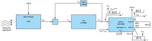
Figure 4. AFE board signal chain.
The laser board generates the optical pulses with a wavelength of 905 nm. It uses four lasers that are driven simultaneously for an increase in beam strength, resulting in a longer measurement range. A PWM signal generated by the FPGA carrier board with programmable pulse width and frequency is used to control the lasers. The signal is generated on the FPGA as LVDS to make it less susceptible to noise as it travels from the FPGA to the laser board through the DAQ board and the ribbon cable connecting the DAQ and the laser boards. The drive signal can be fed back to one of the ADC channels for time of flight reference. An external power supply is used to power the lasers. The design complies with International Standards IEC 60825-1:2014 and IEC 60825-1:2007 for a Class 1 laser product.
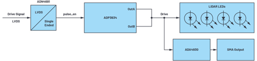
Figure 5. Laser board signal chain.
Both the AFE and laser boards require optics for long distance operation. The system was proven to operate at 60 m using fast axis collimators1 for the laser diodes that narrow the vertical FoV to 1° while keeping the horizontal field of view unchanged, and an aspherical lens for the receive side.
HDL Reference Design
The HDL design constitutes the primary interface to the hardware and implements all the logic to transfer data from the JESD link to the system’s memory, drive the lasers, synchronize the receiver and transmitter for accurate time of flight measurement, and implement the communication interfaces to all the components in the hardware design. Figure 6 shows a simplified block diagram of the HDL design. The generic architecture of the ADI’s HDL reference designs makes the framework scalable and more accessible to port to another FPGA carrier. The design is using the Analog Devices JESD204B framework2 along with several SPI and GPIO interfaces to receive data from the AD9094 ADC and to control all the devices on the prototyping platform.
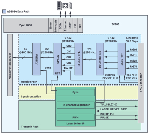
Figure 6. HDL design block diagram.
The JESD204 link is configured to support four data converters (M) using four lanes (L) with a lane rate of 10 Gbps for a converter resolution of eight bits. The device clock, which will be the same as the reference clock for the high speed transceivers, is set to 250 MHz and is provided by the DAQ board. The link is running in Subclass 1 mode, which ensures deterministic latency between the high speed converter and FPGA.
One of the biggest challenges of a LIDAR system is how to synchronize various functions to the transmitted pulse and how to process just the necessary amount of data, received from the high speed ADC. To address this, the HDL design contains an IP that provides the required logic to generate a laser pulse, control the internal multiplexers of the TIAs and provides a back-pressure for the DMA. All these control functions are synchronized with the transmitted pulse, so the system doesn’t have to save all the raw digitized high speed data stream. This way, the overall data rate of the system is highly reduced.
Software
The key points that define the software stack for the LIDAR platform are free and open source. The user gets through them the “freedom to run, copy, distribute, study, change, and improve the software.”3 Starting from the Linux® kernel and continuing with the user space tools, everything respects this.
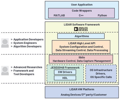
Figure 7. Software stack.
The software drivers implemented in the kernel initialize the hardware components and expose to the user all their useful functionalities. Most of these drivers are part of the Industrial I/O (IIO) Linux subsystem.4 The drivers are all platform agnostic, so hardware changes, including carrier ones (for example, migrating from a Xilinx® FPGA to an Intel® one), do not require them to be changed.
To ease the development of software interfacing IIO devices, ADI has developed the libiio library.5 It abstracts the low level details of the hardware and provides a simple yet complete programming interface that can be used for advanced projects. The various available libiio back ends (for example, local, network, USB, serial) make possible the usage of IIO devices locally and remotely from applications running on different operating systems (for example, Linux, Windows®, macOS®).
The IIO oscilloscope, developed by ADI, is an example of an application that uses libiio to interface with IIO devices and can be used during the system evaluation stage. The tool can capture and plot data in different modes (for example, time domain, frequency domain, constellation, cross-correlation), transmit data, and allow users to view and modify the settings of the detected devices.
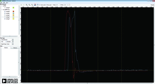
Figure 8. IIO oscilloscope capture window displaying LIDAR data.
While libiio provides a low level programming interface, in most cases, users expect a platform-specific API that abstracts the low level driver calls and exposes a set of functions to access and configure the various system parameters and stream data from the system. For this reason, the LIDAR prototyping platform comes with a specific API with bindings for popular frameworks and programming languages such as C/C++, MATLAB®, or Python®,6 enabling users to interface with the system using their preferred programming language and focus on algorithms and applications, which is the value proposed to their customers.
Conclusion
In any system design, when the architecture is being established and design decisions are being made, there is a certain degree of ambiguity. This represents the risk that the system will not work or perform as expected after being built, resulting in multiple design cycles, increased development cost, and longer time to market for a product. Being built on pre-engineered systems intended to interoperate with each other, reference designs reduce risk and improve overall predictability and reliability as compared to using a custom, one-off design built from scratch. Using a reference design as a starting point in the planning process helps bring new designs to market faster and helps ensure there are fewer surprises and problems. System designers are always seeking reference platforms to prove out the design decisions, thus reducing the risk and improving reliability. Starting a project with clear and standardized design options facilitates the planning process. It does so by using a common language to help align goals, encourage cooperation and participation across multiple functions, and make it easier to evaluate the trade-offs between design goals.
The LIDAR prototyping platform tries to meet these needs by providing open-source hardware and software designs that can be referenced in the initial system architecture phases. The hardware platform and the software stack can be used through all the phases of product development, from initial system evaluation, development, and integration into the final product. The contents of the reference design such as engineering drawings and a BOM provide a head start in getting to buildable, legal, and localized design system. This shortens the design cycle and likely saves money in the process. The modular hardware design allows various configuration options to meet the specific application requirements, while the open-source software stack, based on industry-standard frameworks and programming languages, and accompanied by application examples, allows customers to focus on developing the applications that bring value to their products without having to spend effort on the low level portions of the stack.


UK Enters ‘Golden Age of Nuclear’
Anybody know why it takes from 2025 to mid 2030's to build a factory-made SMR, by RR? Ten years... has there been no demonstrator either? Do RR...