It is the latest work from Prof Andre Geim and Prof Kostya Novoselov, based at Manchester University, who after creating the first graphene sheet using scotch tape now wish to speed up progress on potential applications of the material.
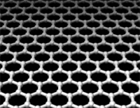
Graphene, which is a single-layered sheet of carbon atoms, has excellent electrical conductivity and very low resistance owing to its hexagonal lattice arrangement of atoms.

However, a single graphene sheet actually conducts charge so well that it is difficult to make the current stop. This is a crucial stumbling-block if the material is ever going to be used for microelectronic devices such as transistors that act to control the flow of current to perform tasks and computations.
To achieve this one must be able to create an electronic band gap, or break in electron energy levels, which essentially turns the material into a semiconductor.
‘Bilayer graphene has this very wonderful property in that a [band] gap can be opened in the spectrum if you apply a voltage perpendicular between the two layers,’ said Novoselov. ‘Not that many materials exist where you can control the opening of the band gap by applying an electric field.’
However, as Novoselov explained, to make use of this property you need to be able to control these states and switch between gapless and gap states — an ability referred to as nematic phase transition.
The team created ultra-high-quality bilayer graphene by suspending single layers in a vacuum. This way, most of the unwanted scattering mechanisms for electrons in graphene could be eliminated, thus enhancing the effect of electron-electron interactions.
Observing current passing though its simple bilayer set-up, the team found complex behaviour involving strongly anisotropic, or directionally dependent, interactions between electrons.
The bottom line, Novoselov said, is that the behaviour was highly consistent with the nematic phase transition phenomenon the team was looking for.
’It’s a new opportunity — we’ve never had a material like this before where you change the gap directly. It’s like having silicon that you can suddenly switch into a metal from being a semi-conductor.’
Novoselov added that further experiments will be needed to fully characterise the properties of the bilayer, then it will be up to engineers to take these properties and build devices. He urged a creative, fresh-thinking approach to this.
‘Rather than fitting this material into old technologies it’s probably worthwhile creating a completely new technology and architecture for itself.’


Poll: Should the UK’s railways be renationalised?
I _do_ remember British Rail - and that it was <i>literally</i> a national joke https://youtu.be/zV2lmSDKvO8