
Advances in automotive technology have significantly increased the electronic content of modern automobiles to enhance safety, improve the driving experience, enrich entertainment functions, and diversify the power and energy sources. We continue to commit engineering resources to improving power management solutions for the automotive market. Many of the technologies from that effort have resulted in significant advances in power supply efficiency, compactness, robustness, and EMI performance.
Power supplies for automotive applications must perform without failure in the face of harsh conditions - the designer must consider all exigencies, including load dump, cold crank, battery reverse polarity, double battery jump, spikes, and other transients defined in LV 124, ISO 7637-2, ISO 17650-2, and TL82066, as well as mechanical vibration, noise, extremely wide temperature ranges, etc. This article focuses on the critical requirements in automotive power supply specifications and solutions to meeting automotive specifications, including:
- Automotive input transients
- Input voltage range
- Output voltage/current
- Low quiescent current (IQ)
- Electromagnetic interference (EMI)
Harsh Automotive Environments
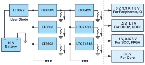
These regulators feature ultralow quiescent current, extending battery run time for always-on systems. Low noise power conversion technology minimises the need for costly EMI mitigation, as well as design and test cycles to meet stringent automotive EMI standards. For many criticalfunctions that must ride through cold crank events, the LT8603 multichannel low IQ buck regulators with a built-in pre-regulation boost controller delivers a compact solution with at least three regulated voltage rails. The LT8602 can deliver four regulated voltage rails required for many advanced drive assistance system (ADAS) applications, such as collision warning, mitigation, and blind spot monitoring.
Figure 2 shows a traditional automotive electrical system where the engine drives an alternator. The alternator is essentially a 3-phase generator, with its ac output rectified by a full diode bridge. The output of this rectifier is used to recharge a lead-acid battery and power 12V circuits and devices. Typical loads include the ECU, fuel pump, brakes, fan, air conditioner, sound systems, and lighting. Increasing numbers of ADAS are addedto the 12V bus, including peripherals, I/Os, DDRs, processors, and their power supplies.
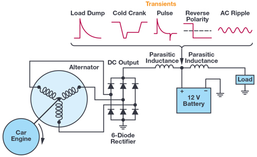
Electric cars change the picture somewhat. The engine is replaced with an electric motor, where a dc-to-dc converter converts a 400V high voltage lithium-ion (Li-Ion) battery stack to 12V, instead of an alternator. Nevertheless, traditional 12V alternator devices are here to stay, along with their transient pulses - including fast pulses.
An engine runs at its peak efficiency in a narrow range of rpms, so the steady state output of the alternator and the battery voltage are relatively stable,say ~13.8V, under most conditions (more about that below). Every circuit powered directly from the car battery must run reliably over the range of 9V to 16V, but robust automobile electronic designs must also operate during outlier conditions that will inevitably occur at the most inconvenient time.
Although output of the alternator is nominally stable, it is not stable enough to avoid the need for conditioning before it powers the vehicle’s other systems. Unwanted voltage spikes or transients are harmful to downstream electronic systems and, if not properly addressed, can cause these systems to malfunction or cause permanent damage. In the past few decades, many automotive standards such as ISO 7637-2, ISO 16750-2, LV 124, TL82066 have been produced to define the spikes and voltage transients that automotive power supplies will face, and set design expectations.
One of the most critical and challenging high voltage transients is load dump. In automotive electronics, load dump refers to the disconnection of the vehicle battery from the alternator while the battery is being charged. During a load dump transient, the excitation field of the alternator remains high given its large time constant - the alternator still outputs high power even without the load. A battery is a bigcapacitor and will normally absorb the extra energy, but when it is disconnected due to a loose terminal or other issues, it can no longer provide this service. As a result, all the other electronics see the voltage surge and must be able to survive load dump events. An unsuppressed load dump could generate voltages upward of 100V. Thankfully, modern car alternators use avalanche-rated rectifier diodes,limiting the load dump voltage to 35V - still a significant diversion from the norm. A load dump event can last up to 400ms.
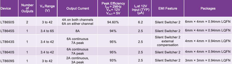
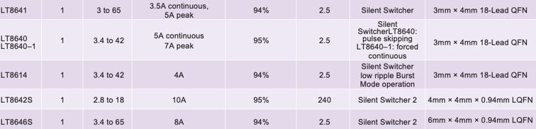
Another high voltage event is jump-start. Some tow trucks use two batteries in series to assure effective jump starts to revive a dead car battery, so an automobile’s circuits must survive the doubled nominal battery voltage of 28V for a couple of minutes. Many ADI high voltage step-down regulators, such as the Silent Switcher® and Silent Switcher 2 families, including the LT8650S and LT8640S (Table 1) operate up to 42V, exceeding this requirement. In contrast, lower voltage rated options would require a clamp circuit, adding cost and lowering efficiency. Some Analog Devices regulators, such as the LT8645S and LT8646S, are rated for 65V to accommodate truck and airplane applications, where a 24V system is the norm.
Table 1. Silent Switcher and Silent Switcher 2 Monolithic Buck Regulators for Automotive Applications
Another voltage transient occurs when a driver starts an automobile and the starter draws hundreds of amperes of current from the battery. This pulls down the battery voltage for a short period of time. In a traditional automobile, this happens only when the car is started by the driver - for instance, when one starts a car to drive to the supermarket and starts it again to drive back home. Inmodern automobiles with start-stop features to save fuel, start-stop events can occur a number of times on that supermarket trip - at every stop sign and every red light. The additional start-stop events put significantly more strain on the battery and starter than in a traditional automobile.
Furthermore, if a start event happens on a cold morning, the starter draws more current than at higher ambient temperatures, pulling the batterydown to 3.2V or lower for around 20ms - this is called cold crank. There are functions that must remain active even in cold crank conditions. The goodthing is that, by design, such critical functions typically do not require significant power. Integrated solutions, such as the LT8603 multiple channelconverter, can maintain regulation even if their inputs drop below 3V.
ISO 7637-2 and TL82066 define many other pulses. Some have higher positive or negative voltages but also higher source impedances. Those pulses have relatively low energy compared to the events described above, and can be filtered or clamped with proper selection of input TVS.
An Ideal Diode Satisfies Automotive Immunity Norms
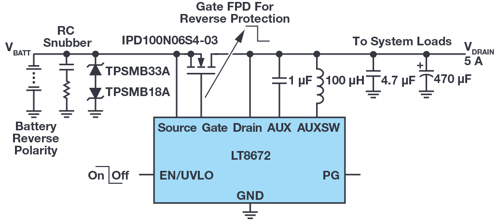
The active rectifier controller LT8672, featuring high input voltage rating (+42V, −40V), low quiescent current, ultrafast transient response speed, and ultralow external FET voltage drop control, provides protection in 12V automotive systems with extremely low power dissipation.
Battery Reverse Polarity
Whenever the battery terminals are disconnected, there is a chance the car battery polarity is reversed by mistake and the electronic systems can be damaged from the negative battery voltage. Blocking diodes are commonly placed in series with supply inputs to protect against supply reversal, but blocking diodes feature a voltage drop, resulting in an inefficient system and reducing the input voltage, especially during a cold crank.
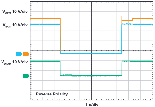
The LT8672 is an ideal diode replacement to the passive diode to protect the downstream systems from the negative voltages, as shown in Figure 3.
Under normal conditions, the LT8672 controls an external N-channel MOSFET to form an ideal diode. The GATE amplifier senses across DRAIN and SOURCE and drives the gate of the MOSFET to regulate the forward voltage to 20mV. D1 protects SOURCE in the positive direction during load steps and overvoltage conditions. When a negative voltage appears in the input side, GATE is pulled to SOURCE when SOURCE goes negative, turning off the MOSFET and isolating DRAIN from the negative input. With its fast pull-down (FPD) capability, LT8672 can quickly turn off the external MOSFET.
Superimposed Alternating Voltage
A common disturbance on the battery rail is a superimposed ac voltage. This ac component can be an artefact of the rectified alternator output or a result of frequent switching of high current loads, such as motors, bulbs, or PWM controlled loads. According to automotive specifications ISO 16750 and LV 124, an ECU may be subjected to an ac ripple superimposed on its supply, with frequencies up to 30kHz and amplitudes of up to 6Vp–p. In Figure 5, a high frequency ac ripple is superimposed on the battery line voltage. Typical ideal diode controllers are too slow to react, but the LT8672 generates high frequency gate pulsesup to 100kHz to control external FETs as needed to reject these ac ripples.
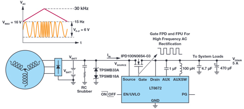
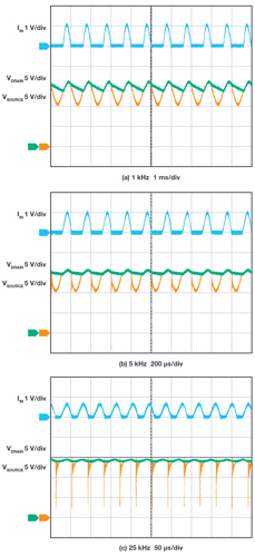
The unique ability of the LT8672 to reject common ac components on a power rail are a function of its fast pull-up (FPU) and FPDcontrol strategy and its strong gate driving capability, where the gate driver is powered by an integrated boost regulator. Compared with a charge pump gate power solution, this boost regulator enables the LT8672 to maintain a regulated 11V voltage to keep the external FET on, while providing strong gate souring current to reduce switching loss for high frequency ac ripple rectification. Its50mA source current capability enables super-fast turn-on of the FET, minimising power dissipation; its 300mA sinking currentcapacity realises fast turn-off, minimising the reverse current conduction. In addition, this significantly reduces the ripple current in the output capacitor. Typical rectification waveforms for a superimposed alternating voltage are shown in Figure 6.
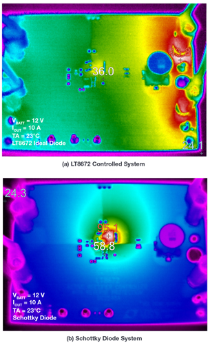
In addition, the LT8672 effectively reduces conduction losses when compared with a traditional Schottky diode solution under the same load conditions. As seen in the thermal images of Figure 7, the solution using the LT8672 is almost 60°C cooler than a traditional diode-based solution. It not only improves the efficiency, but also eliminates the need for a bulky heat sink.
- The disconnection of input power supply when there is inductive load in series or parallel.
- The switching processes of a load influencing the distributed capacitance and inductance of a wire harness.
Some of these pulses could have high voltage peaks. For example, pulse 3a defined in ISO 7632-2 is a negative spike whose peak voltageexceeds −220V, while pulse 3b defines a pulse with maximum peak voltage of 150V, on top of the battery’s initial voltage. Although they feature a large internal impedance and very narrow duration time, downstream electronics could be easily damaged if they see these pulses.
Two properly sized TVSs are installed in the front end to suppress such spikes. In fact, some of the low energy pulses could be absorbeddirectly by filter effect of input capacitor and parasitic wire inductance.
Multiple Rail Regulator Rides Through Cold Crank Events
The LT8602 provides compact solutions for up to four regulated rails (for example, 5V, 3.3V, 1.8V, 1.2V) with an input voltage range from 5V to42V, suitable for functions that do not necessarily need to be on during a cold crank. Otherwise, for functions that must operate even during cold crank - such as the spark plug controller or alarm - solutions like the LT8603 work down to 3V (or lower) inputs.
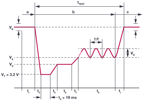
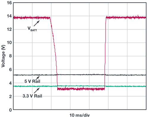
LV 124 has defined the worst case of cold crank, shown in Figure 8. It indicates that the lowest battery voltage can go down to 3.2V and last for 19msat car start-up. This specification challenges applications to keep running as low as 2.5V when faced with the extra diode voltage drop from battery reverse protection in a traditional (non-ideal diode) solution. In a passive diode protection scheme, buck-boost regulators may be required instead ofless complex and more efficient buck regulators to provide a stable 3V supply often required by many microcontrollers.
The LT8672 controller features a minimum input operating voltage of 3V VBATT, enabling the active rectifier to operate through the cold crank pulse with a minimum drop (20mV) between input and output. Downstream power supplies during a cold crank event see an input voltage no lower than 3V. This allows use of a buck regulator with a minimum operating voltage of 3V and low dropout characteristics, such as the LT8650S, to generate a 3V supply.
Like the LT8650S, many ADI automotive ICs feature minimum input voltage rating of 3V.
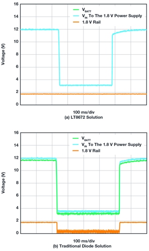
Figure 9 shows the comparison of 1.8V power supply with the LT8672 and with a traditional diode. The step-down regulator works down to 3V. As shown, with a traditional diode, VIN to the buck regulator drops to near 2.7V when the battery voltage VBATT drops to 3.2V, due to high voltage drop of the diode, triggering the UVLO shutdown of the downstream switching regulator, and its 1.8V output collapses. In contrast, voltage remains nearly constantat the LT8672 output during a cold crank event, and the downstream step-down regulator is able to maintain a 1.8V output.
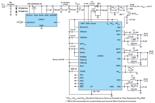
Numerous critical functions require regulated 5V and 3.3V rails, plus sub-2V rails to power content, processor I/O, and core in analogue anddigital ICs. If VBATT drops below its outputs or VIN (MIN), a pure buck regulator would lose regulation if directly powered from VBATT. However, suchcritical functions typically do not require much power, so a highly integrated compact solution can be used, such as the 6mm × 6mm LT8603 quad output, triple monolithic buck converter plus boost controller.
The LT8603’s integrated boost controller works down to below 2V, making it an ideal pre-regulator to its three buck regulators. Figure 10 shows an ADI state-of-the-art solution for these applications that can ride through a cold crank event. The two high voltage buck regulators are powered by the pre-boost converter. When VBATT drops below 8.5V, the boost controller starts switching and the output (OUT4) is regulated to 8V. It can keep the output regulated with the input voltage down to 3V once it is started. Therefore, the two high voltage bucks can ride through the cold crank condition, while providing constant 5V and 3.3V outputs, as shown in Figure 11. Once VBATT recovers to above 8.5V from cold crank, the boost controller simply works as a diode pass through. The high voltage bucks can handle VBATT up to 42V. The low voltage buck is powered from OUT2, providing 1.2V through the cold crank event.
Ultralow IQ Extends Battery Run Time for Always-On Systems
For always-on systems connected to VBATT for weeks or months without a battery recharge, light load and no-load efficiency are, in some cases,more important than full load efficiency. The Analog Devices family of ultralow quiescent current (IQ) devices preserve battery charge while withstanding challenging transient conditions and wide input voltage ranges, from 3V to 42V, and wide temperature ranges. To optimise efficiency and maintain regulation at light loads and no load, the regulator features Burst Mode® operation. Between bursts, all circuitryassociated with controlling the output switch is shut down, reducing the input supply current to a few microamps. In contrast, a typical buckregulator might draw hundreds of hundreds of microamps from VBATT when regulating with no load, draining the battery orders of magnitude faster.
The Burst Mode efficiency at a given light load is mainly affected by the switching loss, which is a function of switching frequency and gate voltage. Because a fixed amount of energy is required to switch the MOSFET on and off, and keep the internal logic alive, a lower switching frequency reduces gate charge losses and increases efficiency. The switching frequency is primarily determined by the Burst Mode currentlimit, the inductor value, and the output capacitor. For a given load current, increasing the burst current limit allows more energy to be delivered during each switching cycle, and the corresponding switching frequency is lower. For a given burst current limit, a larger value inductor storesmore energy than a smaller one, and the switching frequency is lower as well. For the same reason, a bigger output capacitor stores more energy and takes longer to discharge.
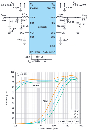
Figure 12 shows the ultralow IQ synchronous buck regulator LT8650S in a solution that features high efficiency over wide input voltage and load current ranges. With integrated MOSFETs, this device can deliver up to 8A total output current at fixed output voltages of 3.3V or 5V. Despite the simple overall design and layout, this converter includes options that can be used to optimise the performance of specific applications in battery-powered systems.
Table 1 lists low IQ monolithic regulators that are well-suited to the automotive market, with inputs up to 42V or 65V. Typical quiescent current for these devices is only 2.5µA, thanks to the low IQ technologies developed by Analog Devices. With minimum turn-on time of 35ns, these regulators deliver 3.3V output voltage from input 42V at switching frequency of 2MHz, which is common in the automotive industry.
Silent Switcher Portfolio Takes Complexity Out of EMI Design
Automotive applications demand systems that do not produce electromagnetic noise that could interfere with the normal operations of other automotive systems. For instance, switching power supplies are efficient power converters, but by nature generate potentially unwelcome high frequency signals that could affect other systems. Switching regulator noise occurs at the switching frequency and its harmonics.
Ripple is a noise component that appears at the output and input capacitors. Ripple can be reduced with the low ESR and ESL capacitors, and low-pass LC filters. A higher frequency noise component, which is much more difficult to tackle, results from the fast switching on and off of the power MOSFETs. With designs focused on compact solution size and high efficiency, operating switching frequencies are now pushed to 2MHz to reduce the passive component size and avoid the audible band. Furthermore, switching transition times have been reduced to the nanosecond realm to improve efficiency - by reducing switching losses and duty ratio losses.
Parasitic capacitance and inductance from both the package and PCB layout play important roles in distributing noise, so if the noise is present, itcan be difficult to eliminate. EMI prevention is complicated by the fact that switching noise covers the domain from tens of MHz to beyond GHz.Sensors and other instruments subjected to such noise could malfunction, resulting in audible noise or serious system failure. Therefore, stringentstandards have been set up to regulate EMI. The most commonly adopted one is the CISPR 25 Class 5, which details acceptable limits atfrequencies from 150kHz to 1GHz.
Passing automotive EMI regulation at high current usually means a complicated design and test procedure, including numerous trade-offs in solution footprint, total efficiency, reliability, and complexity. Traditional approaches to controlling EMI by slowing down switching edges or loweringswitching frequency come with trade-offs such as reduced efficiency, increased minimum on-and off-times, and larger solution size. Alternative mitigation, including a complicated bulky EMI filter, snubber, or metal shielding, adds significant costs in board space, components, and assembly,while complicating thermal management and testing.
Our Silent Switcher technology addresses the EMI issue in an innovative way, enabling impressive EMI performance in high frequency, high power supplies. Second generation, Silent Switcher 2 devices simplify board design and manufacture by incorporating the hot loop capacitors into the packaging. For a buck regulator such as the 42V/4A LT8650S, the hot loop consists of an input capacitor and the top and bottom switches. Other noisy loops include the gate drive circuit and boost capacitor charge circuit. In Silent Switcher 2 devices, the hot loop and warm loop capacitors are integrated into the packaging and laid out to minimise EMI. This reduces the effect of final board layout on the EMI equation, simplifying design and manufacturing. Further peak EMI reduction can be achieved by using the optional spread spectrum frequency modulation feature incorporated into these parts, making it even easier to pass stringent EMI standards.
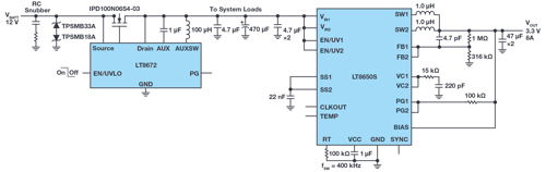
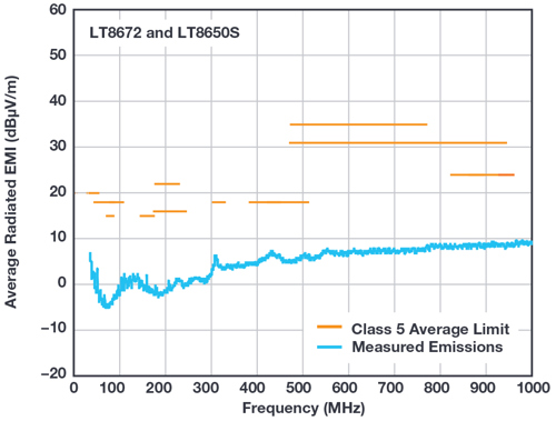
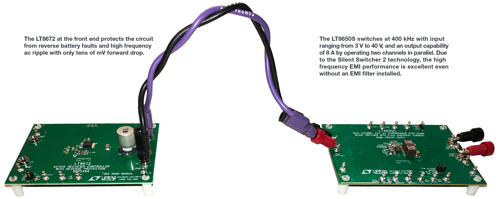
Figure 13 exhibits a low IQ, low noise solution for a high current application for automotive I/Os and peripherals. The LT8672 at the front end protectsthe circuit from reverse battery faults and high frequency ac ripple with only tens of mV of forward voltage drop. The LT8650S switches at 400kHz with input ranging from 3V to 40V, and an output capability of 8A by operating two channels in parallel. Two decoupling capacitors are placed close to theinput pins of the LT8650S. With Silent Switcher 2 technology, the high frequency EMI performance is excellent even without an EMI filter installed. The system passes the CISPR 25 Class 5 peak and average limit with significant margins. Figure 14 shows the radiated EMI average test results over the range of 30MHz to 1GHz, with vertical polarisation. A complete solution features a simple schematic, minimal overall component count,compact footprint, and EMI performance that is immune to changes in board layout (Figure 15).
Conclusion
Automotive applications call for low cost, high performance, reliable power solutions. The cruel under-the-hood environment challenges power supply designers to produce robust solutions, taking into account a wide variety of potentially destructive electrical and thermal events. Electronic boards connected to the 12V battery must be carefully designed for high reliability,compact solution size, and high performance. The Analog Devices device catalogue includes innovative solutions specifically addressing automotive requirements: ultralow quiescent current, ultralow noise, low EMI, high efficiency, wide operating ranges incompact dimensions, and wide temperature range. By eliminating complexity while improving performance, Analog Devicessolutions reduce power supply design time, lower solution costs, and improve time to market.
About the Author
Bin Wu (S’14) was born in Zhejiang, China, 1985. He received his Ph.D. degree in electrical engineering from University of California, Irvine, California in April 2016. From April 2016 to July 2017, he was a post-doctoral research associate in University of Maryland, College Park. After that, he worked at Maxim Integrated, Inc. Since November 2017, he has been an applications engineer with Analog Devices, San Jose. His interests include electrical vehicle power architecture, high power density step-up/step-down dc-to-dc converters, switched capacitor converters, modelling, and renewable energy integration systems. He can be reached at bin.wu@analog.com.
About the Author
Zhongming Ye is a senior applications engineer for power products at Analog Devices in Milpitas, California. He has been working at Linear Technology (now part of Analog Devices) since 2009 to provide application support to various products including buck, boost, flyback, and forward converters. His interests in power management include high performance power converters and regulators of high efficiency, high power density, and low EMI for automotive, medical, and industrial applications. Prior to joining Linear Technology, he worked at Intersil for three years on PWM controllers for isolated power products. He obtained a Ph.D. degree in electrical engineering from Queen’s University, Kingston, Canada. Zhongming was a senior member of IEEE Power Electronics Society. He can be reached at zhongming.ye@analog.com.


Poll: Should the UK’s railways be renationalised?
As long as not subject to political interference they are a piece of critical national infrastructure and should be treated with the strategic...