
Nandin Xu, Product Applications Engineer, Analog Devices
Introduction
Considering that resolvers have outstanding reliability and high precision performance in harsh and severe environments for a very long time, they are widely used in EV, HEV, EPS, inverter, servo, railway, high speed train, aerospace, and other applications where position and velocity information is needed.
Many resolver-to-digital converters (RDCs), such as Analog Devices’ AD2S1210 and AD2S1205, used in previous systems to decode the resolver’s signal to get digital position and velocity data. Interferences and fault issues tend to happen in customers’ systems, and most of the time they want to evaluate the accuracy performance of angle and velocity under the interference conditions, find and validate the root cause, then fix and optimise the system. A high accuracy resolver simulator (which simulates a resolver attached to the real motor at constant speed or position) with fault injection can solve the interference and fault pain-points without setting up a complicated motor control system.
This article will analyse the error contribution in resolver simulator systems and give some error calculation examples to help understand why highprecision is so important in resolver simulators. It will then show the fault case under interference conditions in field applications. Following that will be adescription of how to build a high accuracy resolver simulator with fault simulation and injection functions using the latest high precision products. Finally, it will show some of the resolver simulator’s capabilities.
Error Contributions in Resolver Simulator Systems
First, this section will introduce the ideal resolver structure. Then, five commonly non-ideal characteristics and error analysis methods will be given to help you understand why high precision is necessary in resolver simulator systems.
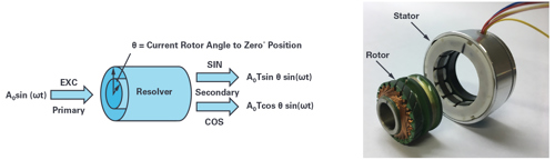
Figure 1. Resolver structure.
The resolver simulator will simulate a resolver, as shown in Figure 1, attached to a real motor at constant speed or position. For classic or variablereluctance resolvers, a rotor and a stator are included. A resolver can be thought of as a special transformer. On the primary side, as expressed inEquation 1, EXC is the excitation sinusoidal input signal. On the secondary side, as expressed in Equation 2 and Equation 3, SIN and COS are themodulated sinusoidal signal at the two outputs.


where:
θ is the shaft angle, ω is the excitation signal frequency, A0 is the excitation signal amplitude, and T is the resolver transformation ratio.
The modulated SIN/COS signals are shown in Figure 2. For constant angular θ in different quadrants, the SIN/COS signal will have in-phase andantiphase cases. For constant velocity, the frequency of the SIN/COS envelope is constant, indicating the velocity information.
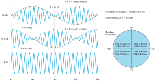
Figure 2. Resolver electrical signal.
For all of ADI’s RDC products, the demodulation signal is expressed in Equation 4. The Type II tracking loop will be accomplished when φ (output digital angle) equals θ (position of the rotor), the resolver angle. In a real resolver system with amplitude mismatch, phase shift, imperfect quadrature, excitation harmonic, and inductive harmonic, any of these five non-ideal conditions may happen and contribute error.

Amplitude Mismatch
Amplitude mismatch is the difference in the peak-to-peak amplitudes of the SIN and COS signals when they are at their peak amplitudes, with 0° and 180° for COS, and 90° and 270° for SIN. Mismatch can be introduced by variations of the resolver windings or by unbalanced gain control of the SIN/COS input. To determine the position error created by amplitude mismatch, Equation 3 can be rewritten as Equation 5.

Where a represents the amount of mismatch between SIN and COS signals, the remaining envelope signal after demodulation can readily be shown, as in Equation 6. When driving the envelope signal to zero in a Type II tracking loop, by setting Equation 6 to equal zero, it is possible to find the position error ε = θ – φ. Then we can receive error information, as shown in Equation 7.


For the realistic case when a is small, the position error is also small, which implies that sin(ε) ≈ ε and θ + φ ≈ 2θ. So, Equation 7 becomes Equation 8, and the error term is expressed in radians.

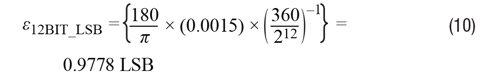
As shown in Equation 8, the error term oscillates at twice the rate of rotation while a maximum error of a/2 is reached at odd integer multiples of 45°. Assume the amplitude mismatch is 0.3%, substitute the variables in Equation 8, and, using an odd integer multiple of 45°, the maximum error will be expressed in Equation 9, where m is an odd integer.

The error, calculated in radians, can be converted to LSBs via Equation 10 when the RDC mode is 12 bits, or about 1 LSB.
Phase Shift
Phase shift refers to both differential phase shift and common phase shift. Differential phase shift is the phase shift between the resolver’s SIN and COS signals. Common phase shift is the phase shift between the excitation reference signal and the SIN and COS signals. To determine the position error created by differential phase shift, Equation 3 can be rewritten as Equation 11.

Where a represents the differential phase shift, the envelop signal remaining after demodulation can be expressed as Equation 12 when the quadratureterm cos(wt)(sin(a)sin(θ)cos(φ)) is ignored. For the realistic case when a is small, cos(a) ≈ 1 – a2/2. When driving this signal to zero in a Type II trackingloop, with Equation 10 set to zero, it is possible to find the position error ε = θ – φ that results. Then we can get error information as shown in Equation13.


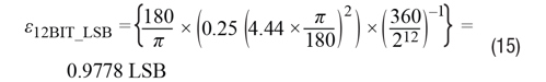
For θ ≈ φ, sin(θ)cos(φ), has a maximum of 0.5 at θ ≈ 45°. So, Equation 13 becomes Equation 14 with the error term expressed in radians.

Assume the differential phase shift is 4.44°, the error, which can be converted to LSBs using Equation 15 when the RDC mode is 12 bits, is about 1 LSB.
When the common phase shift is β, Equation 2 and Equation 3 can be rewritten as Equation 16 and Equation 17, respectively.


Similarly, the error term can be expressed in Equation 18.

Under static operating conditions, common phase shift will not affect the converter’s accuracy, but resolvers at speed will generate speed voltages due to the reactive components of the rotor impedance and the signals of interest. Speed voltages, which only occur at speed and not at staticangles, are in quadrature to the signal of interest. When the common phase shift is β, the tracking error can be approximated as Equation 19, where ωM is the motor speed and ωE is the excitation speed.

As shown in Equation 19, the error is proportional to the resolver speed and phase shift. Thus, in general, it is beneficial to use a high resolver excitation frequency.
Imperfect Quadrature
Imperfect quadrature indicates the two resolver signals that SIN/COS refer to in this situation are not exactly 90° quadrature. This occurs when the two resolver phases are not machined or assembled in perfect spatial quadrature. When β represents the amount of imperfect quadrature, Equation 2 and Equation 3 can be rewritten as Equation 20 and Equation 21.


As before, the envelop signal remaining after demodulation can readily be shown as Equation 22. When you set Equation 22 to zero, assume β is small, cos(β) ≈ 1 and sin(β) ≈ β, it is possible to find the position error ε = θ – φ that results. Then we can receive error information, as shown in Equation 23.


As shown in Equation 23, the error term oscillates at twice the rate of rotation, while a maximum error of β/2 is reached at odd integer multiples of 45°. Compared to the error due to amplitude mismatch, in this case, the mean error is non-zero and the peak error is equal to the quadrature error. From the amplitude mismatch example, when β = 0.0003 radian = 0.172°, this can cause about 1 LBS error in 12-bit mode.
Excitation Harmonic
In all the preceding analysis, it was assumed that the excitation signal was an ideal sinusoid and contained no additional harmonics. In a real-world system, the excitation signal does contain harmonics. So, Equation 2 and Equation 3 can be rewritten as Equation 24 and Equation 25.
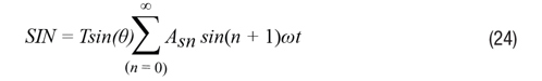
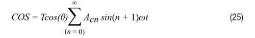
The envelope signal remaining after demodulation can readily be shown, as in Equation 26. Driving this signal to zero in Type II tracking loop.
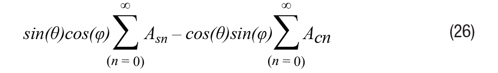
Set Equation 26 to zero and it is possible to find the position error ε = θ – φ that results. Then we can get error information as shown in Equation 27.
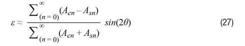
If the resolver excitation has identical harmonics, the numerator of Equation 27 is zero and no position error is incurred. That means the common excitation harmonic has negligible effect on the RDC, even at very large values. However, if the harmonic content is different in SIN or COS, the positionerror incurred has the same functional shape as the amplitude mismatch shown in Equation 8. This will greatly affect the accuracy of the position.
Inductive Harmonic
In the real world, it is impossible to construct a resolver with inductance profiles that are perfect sinusoidal and cosinusoidal functions of position. Normally, the inductances will contain harmonics, and VR resolvers will contain dc components. Thus, Equation 2 and Equation 3 can be rewritten as Equation 28 and Equation 29, respectively, where K0 indicates the dc component.
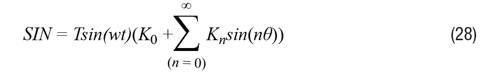
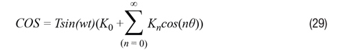
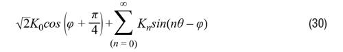
The remaining envelope signal after demodulation can be shown, as in Equation 30.
Driving this signal to zero in a Type II tracking loop, when the harmonic amplitudes are small, Kn <<1 for n >1, the error information ε = θ – φ can be derived from Equation 31.
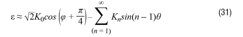
According to the expression, the error is more sensitive to the dc term than the harmonic effect, it is proportional to the inductive harmonic amplitude. In the meantime, the nth inductance harmonic determines the amplitude of the (n – 1)th harmonic of the position error.
Summary of Error Contribution in a Resolver Simulator System
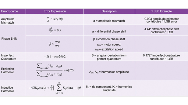
Except for the error source mentioned, the interferent coupled to the SIN and COS lines, amplifier offset error, bias error, etc., can also contribute to the system error. The error source and contribution summary in the resolver simulator system, with the worst example of 1 LSB of 12-bit mode included, are shown in Table 1. Another RDC resolution mode can be calculated by referring to the table.
Table 1. Summary of Error Source and Contribution in a Resolver Simulator System
Fault Types in an RDC System
In real RDC systems, a lot of fault cases can appear. The following sections will show different fault types and some fault signals from field tests, and how the fault type can be simulated when using the resolver simulator solution described in the third section. Except for the fault type mentioned, there may be random interference that leads to another fault, or some faults may happen at the same time.
Misconnection Fault
Misconnection means connected resolver excitation and SIN/COS pairs to RDC SIN/COS input and excitation output pins via incorrect connections. When a misconnection happens, RDC can also decode the angular and velocity information, but the angular output data will show some a jump, like an offset error in DAC output. The misconnection case and result data are shown in Figure 3. Where the first column shows the EXC/SIN/COSpins and output angular, the remaining columns show the misconnection cases.
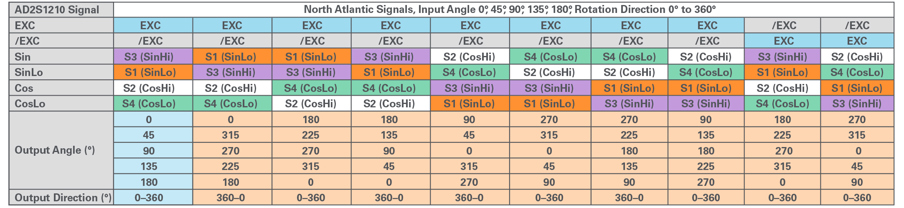
Figure 3. Resolver misconnection and angular output.
Phase Shift Fault
From the error contribution section, we know phase shift contains differential phase shift and common phase shift. Considering the differential phase can be thought of as the difference of common phase shift, in this section, the phase shift fault means the fault caused by common phase shift.
The common phase shift error contribution is shown in Figure 4. Phase 1 is excitation filter delay. Phase 2 is resolver phase shift. Phase 3 is line delay. Phase 4 is SIN/COS filter delay. In a field RDC system, when phase shift error happens, it means the total value of phases 1, 2, 3, and 4 is bigger than44°. Normally, the resolver phase shift error is 10°. In bad cases, the total phase value can reach 30°. For MP consideration, enough phase marginneeds to be left.
When the phase shift for SIN/COS are different, it can cause phase shift mismatch fault. If this happens, angular and velocity accuracy will be affected.
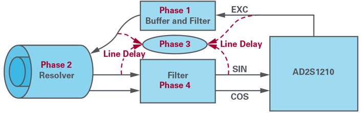
Figure 4. Phase shift error contribution.
Disconnection Fault
Disconnection fault happens when any line of the resolver is disconnected from the RDC platform interface. With the product safety upgrade, line disconnection detection is always mentioned by customers. This fault can be simulated to set SIN/COS to zero voltage. When disconnection happens, LOS/DOS/LOT fault can be triggered in AD2S1210.
Amplitude Mismatch/Exceed Fault
Amplitude mismatch happens when the circuit gain control or resolver ratio of SIN/COS are different, which also means the amplitude value of theSIN/COS envelope is different. When the amplitude is close to AVDD, it will trigger an amplitude exceed fault. For AD2S1210, this is called a clippingfault. A good SIN/COS signal example is shown in Figure 5.
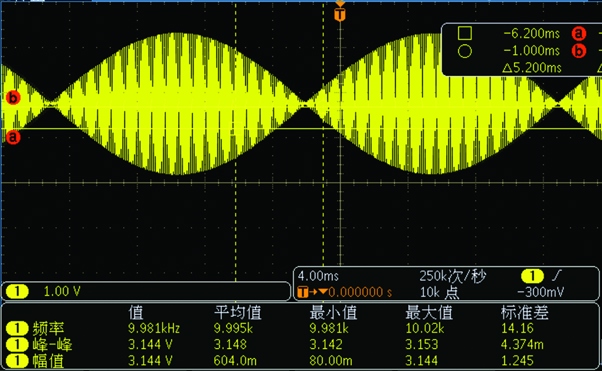
Figure 5. An ideal SIN/COS signal.
IGBT Disturbance Fault
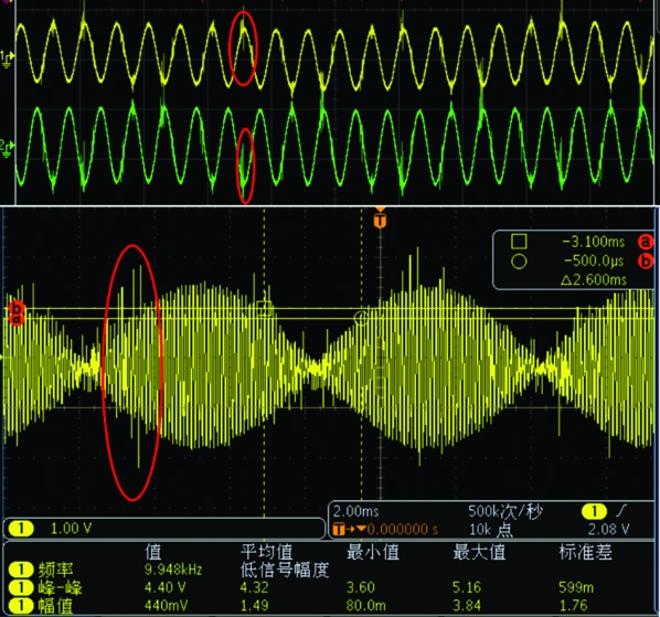
Figure 6. A SIN/COS coupled IGBT disturbance.
An IGBT disturbance means that the interference signal coupled with the IGBT switch on/off effect. When the signal is coupled with the SIN/COS line, position and velocity performance can be affected, the angular value will have a jump, and the direction of the velocity may change. An examplefrom the field is shown in Figure 6, where Channel 1 is the SIN signal, Channel 2 is the COS signal, and the spur indicates interference coupled with IGBT turn on/off.
Velocity Exceed Fault
Velocity exceed fault happens when the electrical velocity is higher than the resolver decode system. For example, in 12-bit mode, the max velocitythat AD2S1210 can support is 1250 SPS, and when the resolver electrical velocity is 1300 SPS, velocity exceed fault will be triggered.
Resolver Simulator System Architecture and Description
From the first section, we know the amplitude and phase error directly determine the performance of decode angular and velocity performance. Luckily, ADI has a vast portfolio of precision products from which to choose and build your resolver simulator system. The following description will show how to build a high accuracy resolver simulator and discuss which parts to choose.
The simulator block diagram as shown in Figure 7 has seven modules to focus on:
- The process control platform for data analysis and control.
- The sync clock generation module generates sync clock for the
- The fault signal generation module generates different fault signals.
- The SIN/COS generation module generates modulated SIN/COS signals as resolver outputs.
- The signal capture module acts as the excitation and feedback signal capture module.
- The SIN/COS output module handles SIN/COS output with buffer, gain, and filter
- The excitation signal input module comes with a built-in buffer and filter
- The power module delivers the supply power for ADC, DAC, switch, amp, components.
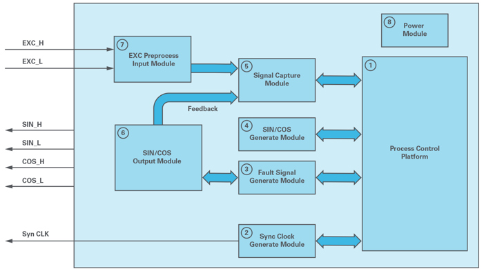
Figure 7. Resolver simulator block diagram.
The resolver simulator system works by having the signal capture module sample the excitation signal from the input module, where the processor will analyse the frequency and amplitude. The processor will calculate the SIN/COS DAC output data code by using the CORDIC algorithm and,through the SIN/COS module, generate the same frequency sinusoidal signal as the excitation input. Then the system will recapture the excitationand SIN/COS signals at the same time, calculate and adjust the SIN/COS phase/amplitude, compensate for the phase error between excitation and SIN/COS so that it equals zero, and calibrate the SIN/COS amplitude to the same level. Finally, the system will generate the modulated SIN/COS signal and fault signal to simulate the angular performance, velocity, and fault case.
The specific signal chain in Figure 8 shows a dual 16-bit sim SAR ADC AD7380 used to capture the excitation and feedback signal when OSR is enabled and a 98dB SNR can be reached. It is very suitable for simultaneous high precision data acquisition for phase and amplitude calibration. Anultra low power, low distortion ADA4940-2 is used as an ADC driver. While a high precision, low noise 20-bit DAC AD5791 is used to generate theSIN/COS and fault signal for lower resolution and lower cost consideration, the AD5541A or AD5781 is recommended to replace the AD5791. Aprecision, selectable gain differential amp, the AD8475, is used as the input/output buffer. Precision, rail-to-rail operational amplifiers with ultralowoffset drift and voltage noise amps, the AD8676 and AD8599, are used to build an active filter and adder circuit. A single-supply, rail-to-rail, 0.8Ω max, dual SPDT, the ADG854, is used to switch and choose the SIN/COS signal, which is then sent to the data capture module.
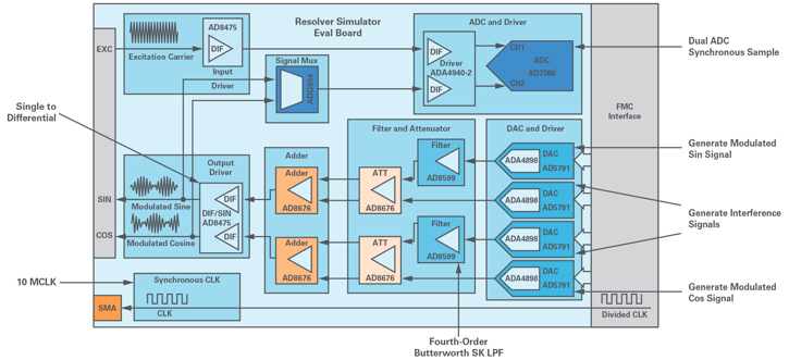
Figure 8. The resolver simulator signal chain.
The whole resolver simulator system is powered through an external 12V adapter with different voltage levels generated by using dc-to-dc converters and LDO regulators. A detailed power supply signal chain is shown in Figure 9. Positive and negative 16V voltages are generated by an ADP5071, but clearer and more stable positive and negative 15V voltages can be generated by using the ADP7118 and ADP7182. These power sources are mainly used to supply power for the DAC-related circuit. Similarly, clear and stable +3.3V, +5V, –5V, and –2V powers are generated by using ADP2300, ADP7118, ADM660, and AD7182. These powers are mainly used to supply power for ADC-related circuits and detailed design requirements.
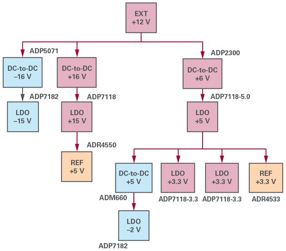
Figure 9. The power supply signal chain.
Resolver Simulator Bench Test and Result
The whole system bench test is shown in Figure 10. It contains a resolver simulator board, an AD2S1210 eval board, and a GUI. The GUI and bench test picture is shown in Figure 11. An AD2S1210 GUI is used to directly evaluate the performance of the resolver simulator, especially velocity and angular performance. Through resolver simulator GUI, velocity, angular performance, and fault signal can be configured.
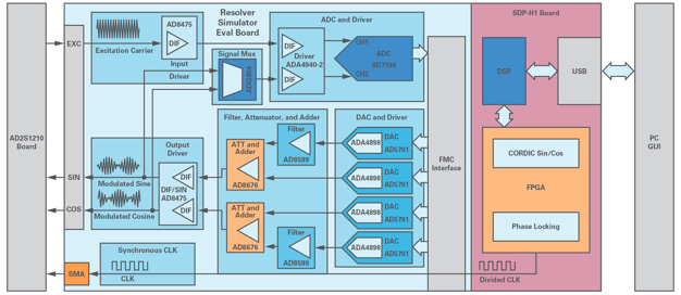
Figure 10. Bench test block diagram.
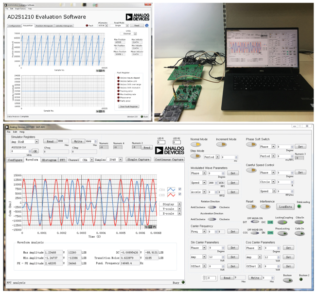
Figure 11. Bench test and GUI.
The INL of angular and velocity performance of a 16-bit AD2S1210 with hysteresis mode disabled is shown in Figure 12.
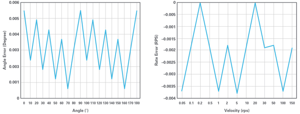
Figure 12. Angular/velocity INL.
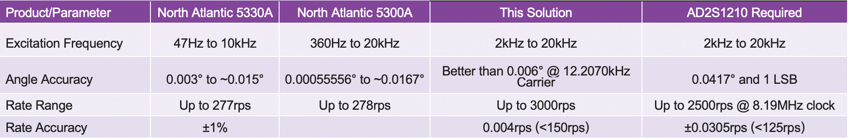
Compared with standard resolver simulator devices, the performance of this solution can be seen in Table 2. A 0.006° angular accuracy can be reached in a real bench test - with 0.0004° in theory when using AD5791 - as well as 3000rps maximal velocity output, 0.004rps velocity accuracy, and can easily meet the 10-bit to approximately 16-bit mode of AD2S1210.
Table 2. Performance Comparison
The fault mode supported in this simulator is shown in Table 3. For phase-related fault, a 0° to approximately 360° range can support a SIN/COS signal. For amplitude-related fault, a 0V to approximately 5V range can support a SIN/COS signal. Exceed velocity, IGBT, disconnection, and other faults can also be simulated by using this solution.
Table 3. Fault Mode and Supported Range

For IGBT fault, one test example is shown in Figure 13. Configure the simulator output to 45°, then add a periodic interference signal to the SIN/COSoutput. As the angular and velocity performance of the AD2S1210 evaluation board GUI shows, the angular performance has fluctuation around 45°, while at the same time the velocity will fluctuate around 0rps.
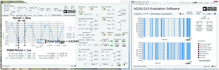
Figure 13. IGBT interference example.
Conclusion
While interference exists in most RDC-related applications, many types of fault can be triggered under serious conditions. When you build your own resolver simulator, follow this solution as it can help you to not only evaluate your system performance under interference, but also calibrate and verify your products as a standard simulator does. Detailed error analysis is very helpful in understanding why precision analogue SIN/COS signals are necessary, and all the fault types discussed in the article can be simulated to help with some functional safety verification.
Analog Devices: www.analog.com
References
Boyes, Geoffrey. “Synchro and Resolver Conversion.” Analog Devices, Inc., 1980.
Hanselman, Duane C. “Resolver Signal Requirements for High Accuracy Resolver-to-Digital Conversion.” IEEE Trans.Ind. Electron., Vol. 37, No. 6, Dec. 1990.
Lynch, Michael. “High Precision Voltage Source.” Analog Devices, Inc., Oct. 2017.
O’Meara, Shane. AD7380 evaluation kits. Analog Devices, Inc., 2019.
Symczak, Jakub, Shane O’Meara, Johnny Gealon, and Christopher Nelson De La Rama “Precision Resolver-to-Digital Converter Measures Angular ” Analog Devices, Inc., Mar. 2014.
Acknowledgements
Many thanks to ADI intern Edward Luo and applications engineers Shane O’Meara, Steven Xie, Karl Wei, and Michael Lynch for their advice and support in the design and test efforts required for this article.
About the Author
Nandin Xu is a product applications engineer at Analog Devices in Shanghai, China. He is responsible for technical support for RDC, isolated modulators, and precision DAC products across China. He joined ADI in 2013 after graduating from Huazhong University of Science and Technology in Wuhan, China with a master’s degree in control science and control technology. In his spare time, he is a super fan of basketball and soccer. He can be reached at nandin.xu@analog.com.


Poll: Should the UK’s railways be renationalised?
The term innovation is bandied about in relation to rail almost as a mantra. Everything has to be innovative. There is precious little evidence of...