
Significantly, the device can recognize specific kinds of polarized light and accordingly send the signal in one direction or another.
Described in the journal Science, the findings are said to offer a new way to precisely manipulate light at the subwavelength scale without damaging a signal that could carry data, making possible a new generation of on-chip optical interconnects that can funnel information from optical to electronic devices.
‘If you want to send a data signal around on a tiny chip with lots of components, then you need to be able to precisely control where it’s going,’ said co-lead author Balthasar Müller, a graduate student at the Harvard School of Engineering and Applied Sciences (SEAS). ‘If you don’t control it well, information will be lost. Directivity is such an important factor.’
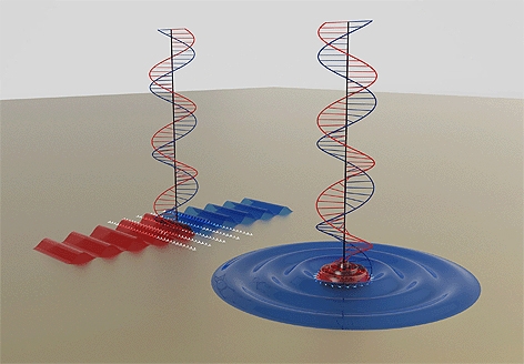
The coupler transforms incoming light into a wave called a surface plasmon polariton, a surface ripple in the sea of electrons that exists inside metals.
Previously, it has been possible to control the direction of these waves by changing the angle at which light strikes the surface of the coupler.
‘‘This was a major pain,’ said Müller in a statement. ‘Optical circuits are very difficult to align, so readjusting the angles for the sake of routing the signal was impractical.’
With the new coupler, the light needs to come in perpendicularly, and the device does the rest because it reads the polarization of the incoming light wave—which might be linear, left-hand circular, or right-hand circular—and routes it accordingly. The device can also split apart a light beam and send parts of it in different directions, allowing for information transmission on multiple channels.
The coupler consists of a thin sheet of gold covered with tiny perforations. The precise pattern of these slits is key to the solution.
‘The go-to solution until now has been a series of parallel grooves known as a grating, which does the trick but loses a large portion of the signal in the process,’ said principal investigator Federico Capasso, Robert L. Wallace Professor of Applied Physics and Vinton Hayes Senior Research Fellow in Electrical Engineering at Harvard SEAS. ‘Now perhaps the go-to solution will be our structure. It makes it possible to control the direction of signals in a very simple and elegant way.’
Because the new structure is so small—each repeating unit of the pattern is smaller than the wavelength of visible light—the researchers believe it should be easy to incorporate the design into novel technologies, such as flat optics.
Müller and Capasso were joined on this work by co-lead author Jiao Lin, a former SEAS postdoctoral fellow who is now at the Singapore Institute of Manufacturing Technology; and coauthors Qian Wang and Guanghui Yuan, of Nanyang Technological University, Singapore; Nicholas Antoniou, Principal FIB Engineer at the Harvard Center for Nanoscale Systems; and Xiao-Cong Yuan, a professor at the Institute of Modern Optics at Nankai University in China.


Poll: Should the UK’s railways be renationalised?
I _do_ remember British Rail - and that it was <i>literally</i> a national joke https://youtu.be/zV2lmSDKvO8