A method for engraving a structured metal coating into an optically-active semiconductor allows more light through while preventing reflections and allowing electrical charge to flow
A novel method for creating a structured surface on metal is the key to a transparent yet electrically-conducting coating that could improve the performance of electronic devices that convert light into current and vice-versa. Called MacEtch, the process has helped researchers from the University of Illinois at Urbana-Champaign to create a surface that allows 90 per cent of incident light through; around 20 per cent more than the bare surface of ther component.
The film is in fact an anti-reflection coating, which allows light through without impeding the flow of current to and from the underlying optoelectronic component. Team leader Daniel Wasserman explained that the patterning of the film’s surface takes the form of an array of microscopic pillars similar to those found on the surface of as moth’s eye. This pattern had previously been found to ‘beat’ a mathematical function called the Fresnel Equation, which governs how light is reflected from and refracted and transmitted through the interface between transparent and opaque materials. “these tiny nanopillars can ‘beat’ the Fresnel equations at certain wavelengths and angles. tiny nanopillars which can ‘beat’ the Fresnel equations at certain wavelengths and angles,’ Wasserman said.
But although the moth-eye pattern improves light transmission, they tend to hinder electrical transmission.
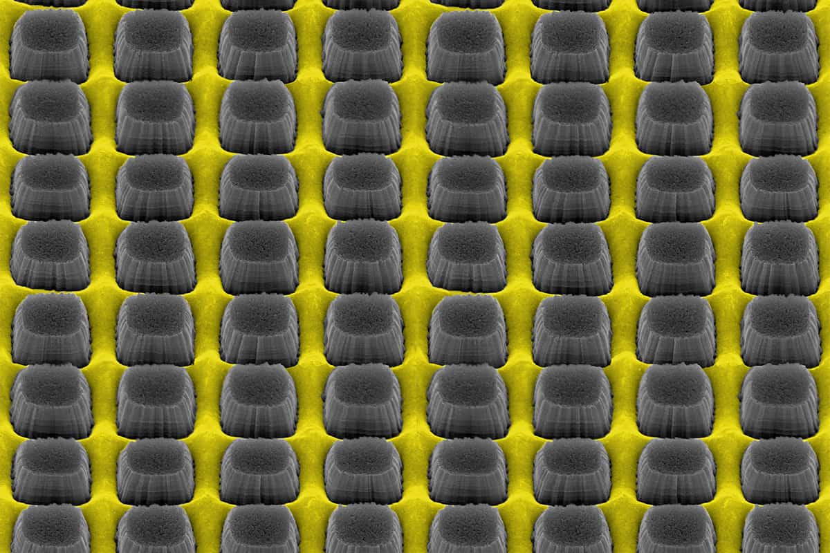
(image courtesy of Dan Wasserman)
In a paper in the journal Advanced Materials, Wasserman and the team explain how they used MacEtch, which was developed by fellow Illinois researcher Xiuling Li, to engrave a metallic coating onto a semiconductor, creating nanopillars with gaps between them smaller than the wavelength of incident light. The metal covers about half the surface area of the semiconductor, but “enhance the optical transmission while the metal film offers electrical contact. Remarkably, we can improve our optical transmission and electrical access simultaneously,” said Runyu Liu, a graduate researcher at Illinois and a co-lead author of the work.
As the metal is engraved into the semiconductor, the team refers top it as a ‘buried’ coating. Adjusting the size of the grating formed by the pillars and the depth the coating is buried fine-tunes the properties of the component. “We are looking to integrate these nanostructured films with optoelectronic devices to demonstrate that we can simultaneously improve both the optical and electronic properties of devices operating at wavelengths from the visible all the way to the far infrared,” Wasserman said.


Glasgow trial explores AR cues for autonomous road safety
They've ploughed into a few vulnerable road users in the past. Making that less likely will make it spectacularly easy to stop the traffic for...