It’s fair to say that over the past few years much of the hype surrounding 3D printing has given way to a more considered and sensible notion of where the technology fits in.
While not so long ago some warned that so-called additive techniques would usurp incumbent manufacturing processes, today they are increasingly seen as complementary: another tool in the toolbox.
But according to Prof Richard Hague, director of the EPSRC centre for additive manufacturing, fundamental breakthroughs are on the horizon that could ultimately help realise some of the more exotic predictions that have been made for the technology.
We’re not just making clever shapes but we’re making them do somethingProf Richard Hague, Director, EPSRC Centre for additive manufacturing
Based at Nottingham University, Hague’s 70-strong team of researchers is making something of a name for itself in one of additive’s most exciting vanguards: the field of multifunctional 3D printing, or 4D printing as it’s sometimes called.
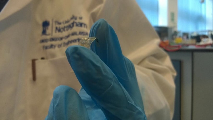
While existing systems typically use just one material, the idea is that multifunctional printers will produce fully functional components from multiple materials, both metals and plastics. It sounds fanciful, but the group has already made significant progress and such techniques could, it is believed, one day enable manufacturers to print entire electronic devices – such as mobile phones – in one go.
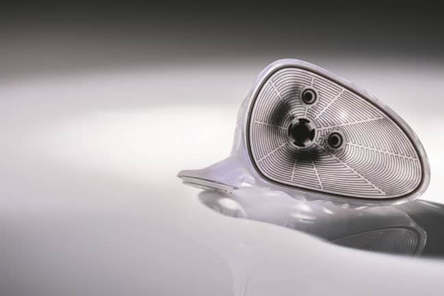
“We’re not just making clever shapes but we’re making them do something.” he told The Engineer. “We’re looking at next-generation multifunctional additive manufacturing, not just printing single materials but putting conductives or pharmaceuticals in the structure.”
Hague and his group have a long track record in the field. Before setting up the EPSRC centre just more than two years ago, he led Loughborough University’s Additive Manufacturing research group, which has itself made a number of significant advances, including the development of software aimed at helping designers to exploit the full advantages of additive techniques.
But the feel and purpose of the Nottingham facility is very different.
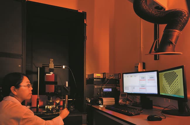
Where the Loughborough lab was home to a large group of engineers and numerous chunks of recognisably industrial equipment, Hague’s current home looks more like a pure science lab. Mechanical engineers are outnumbered by white-coated chemists and physicists, while the benches and worktops are adorned with a variety of unusual looking experimental systems.
It is, said Hague, “a very different beast” and the result of a deliberate decision to step back from the industrial coal face and concentrate instead on advancing the underlying materials science, something that he feels has been lacking in the past, and that has potentially held back the technology. “People working in industry are doing really great stuff but I think historically there hasn’t been enough science and basic understanding,” he said.
Hague admits that stepping down the so-called Technology Readiness Levels (TRLs) to focus on technology with less immediate commercial relevance is an unconventional move, but believes that in the long term the benefits for the technology, and for the UK, could be significant.
“A lot of the original systems – stereolithography, etc – were developed in companies and all the development and IP was held by those companies,” he said. “Universities would buy the systems, work on new materials, clever designs and all that kind of stuff, but in terms of the basic processes themselves all the IP is held overseas. One of the reasons we wanted to go down the TRLs was to develop our own IP for the UK, exploit that and take it forward, and then canter back up the TRLs later on.”
Showing The Engineer around his state-of-the-art lab, Hague’s breezy enthusiasm makes it sound like it’s going to be a walk in the park. “Build a structure, build a function, print it all in one go and off you trot,” he said. The reality is that his team is entering largely unchartered territory, and there are some major technical challenges ahead.
Much of the group’s research is based around advanced jetting technologies rather than the powder-based sintering techniques more familiar to industry. “With powder-based technology, you’re basically laying a whole layer of powder, and there’s no differentiation of materials on that layer,” explained Hague. “With jetting, you can selectively deposit different materials.”
The advantages are obvious, but one of the key challenges is actually getting the material out of the jetting head. The water-like viscosity required to achieve this, explained Hague, means that conventional polymers, for instance, are unsuitable. The group therefore spends a lot of time tweaking the properties of materials: one of the reasons there are so many chemists in the department.
Another potential solution to this problem is a technique known as reactive jetting, which, rather than jetting polymers directly, enables them to be created at the point of deposition. “Because some polymers are too viscous when polymers [you can’t melt them and then jet them], you might want to jet the monomers, which are often very fluid. You can jet two monomers and a catalyst and at the point at where they drop together you can get in-situ polymerisation,” Hague explained.
Drug delivery
The pharmaceutical industry is eyeing up the potential of multifunctional printing.
Despite the fundamental nature of the team’s work, there is nevertheless a high level of industrial interest, and some of it from quite unexpected quarters. Indeed, while the centre’s focus on printed electronics remains a major driver, it is also undertaking work for the pharmaceuticals industry, which, said Hague, is very interested in the 3D printing of drugs. “At the moment, drugs are banged out in the gazillions and you might want to do lower volumes or localised production,” he explained. What’s more, multifunctional techniques could also enable the properties of drugs to be altered. “You might also want to have different drugs at different places within the pill that elute at a different rate.”
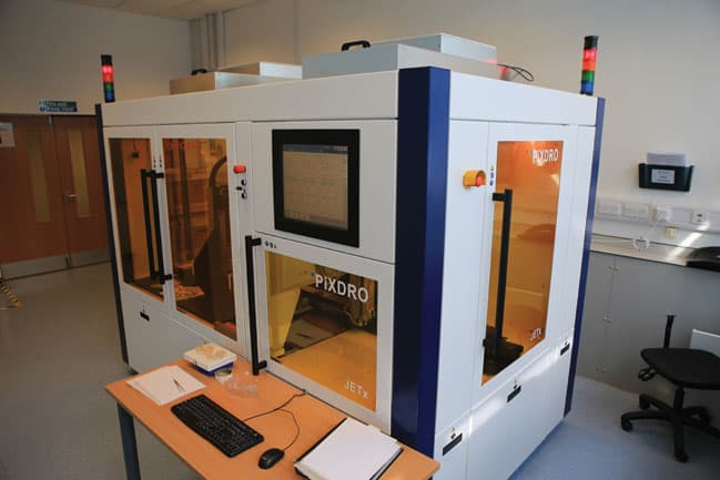
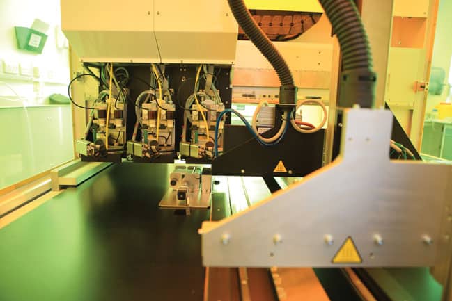
Meanwhile, the quest for new ‘jettable’ materials is a painstaking and complex process in which different formulations are trialled and qualified on a range of systems of increasing cost and complexity before finally being trusted on what’s currently the lab’s ultimate machine: a multifunctional £1m testbed known as Jetx3D.
Purpose built for the centre by Dutch inkjet specialist Roth and Rau, the machine, known internally as ‘The Toucan’, is effectively a 3D adaptation of technology originally developed for 2D-printed electronics. Specially commissioned by Hague’s team, the system has six piezo-electric print heads each equipped with 128 nozzles and can jet a range of materials, including conductive materials such as silver and other metals that are deposited within a carrier material.
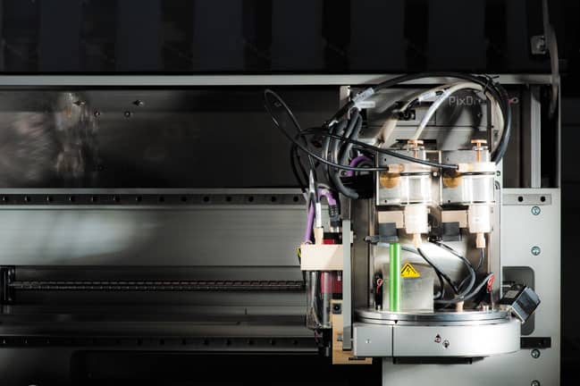
It is a unique piece of equipment, said Hague, literally the only one of its kind in the world, and it’s expected to help drive some major breakthroughs in multifunctional printing. However, the team is now excitedly awaiting the arrival of an even more advanced piece of equipment that will take the ability to jet metal to the next level.
The Metaljet machine, which is being developed for the group by Dutch mechatronics specialist Demcon, is based on technology developed by yet another Dutch firm, Océ, a jetting specialist owned by Canon. Océ’s technology centres around a highly innovative drop-on-demand print head that works at up to 1,800°C and is capable of directly depositing high-temperature metallics in 3D.
Able to jet different metals from its four printheads, the new system is the first of its kind in the world, and, according to Hague, represents a major step towards the dream of 3D printing real electronic devices. “Currently, all of the printed electronics stuff is done with nano-flakes of silver that are loaded into a carrier material that you deposit and then evaporate off the carrier materials. This is very different. Instead of depositing particles suspended in a carrier solvent, it is actually jetting the actual bulk metal and so conductivity is not compromised and no secondary processing is required.”
But despite the primary focus on exotic techniques such as this, Hague is also keen to build on his group’s hard-won expertise in more established areas of additive technology. To this end, he and a number of colleagues have established Added Scientific, a spin-out company aimed at helping organisations without their own corporate research laboratories to build up their competence in additive techniques.
Since its launch, and in stark contrast to the difficulties Hague had enthusing industry about additive earlier in his career, the company has been inundated with work. “The kind of companies we work with now – 10 years ago I would have bitten your hand off,” he said. “We’re flooded with companies, and we don’t want to turn away the industrial interest. We want to have the industrial interest so we can take through the multifunctional stuff in a few year’s time.”
This high level of interest is a sure sign that additive is becoming more and more of a mainstream process. But is it really any closer to becoming the silver-bullet process that some claim will fundamentally reshape manufacturing?
“I would like to say that 3D printing could be used for everything,” said Hague, “and we push at a research level that we want to use [it] to do everything. But in reality you’re going to have to do some post-processing and some joining with other technology. Generally, additive will be a tool in the toolbox and it won’t be used to make absolutely everything of every component ever – we will be able to make systems on these additive processes but whether everything in the phone, car or plane be 3D printed? Probably not. It’s going to be used where appropriate.”
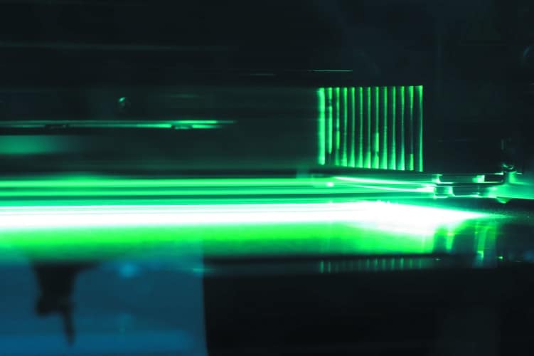
It’s not all about jetting
Using a technique known as two-photon lithography, the Nottingham team hopes to pioneer the production of nanoscale multifunctional components.
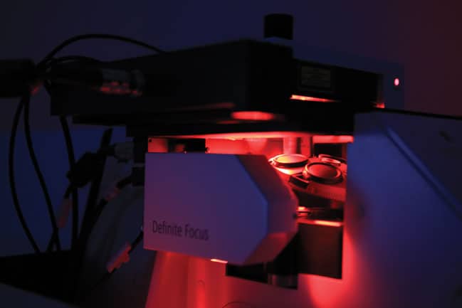
Tucked away in a quiet side room of Hague’s laboratory, a technique is under development that could enable the production of functional 3D components that are smaller than a grain of sand.
Like conventional stereolithography, the process, which is known as two-photon lithography, uses light to cure a liquid resin. However, in this case the resin is engineered so that the curing reaction can only be kicked off by two photons of light. This enables extreme levels of precision and, Hague said, makes it possible to produce nanoscale structures at high resolution in comparison with standard additive manufacturing methods.
This is challenging in its own right. But the team has also thrown optical tweezers into the mix, essentially a laser-based technology that can be used to place individual particles at particular sites and tailor the properties in specific areas of the structure. “For instance,” said Hague, “by embedding gold and silver particles in a particular area, you can tailor conductivity to make devices such as sensors.”
Able to produce structures as small as 150nm, the system is expected to have applications in areas such as optics, metamaterials and biological constructs.


Poll: Should the UK’s railways be renationalised?
I think that a network inclusive of the vehicles on it would make sense. However it remains to be seen if there is any plan for it to be for the...