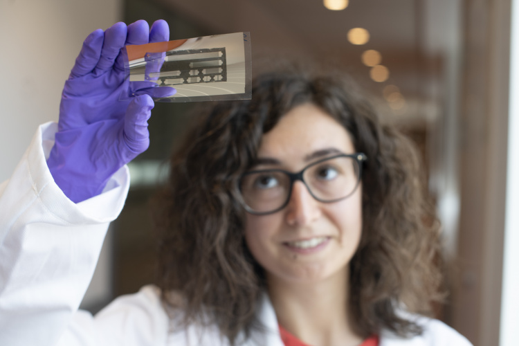
Every electronic device needs to connect its components with conductive pathways. For most, the answer is to form the appropriate pattern in metal, either by selectively removing metal from a film or printing with metal inks onto an insulating substrate. Both techniques have drawbacks, however: metal inks are expensive and removing material to make a pattern requires etching using hazardous chemicals.

Tackling this problem, a team of chemists from the University of Warwick has devised a method using no toxic chemicals and avoiding metal wastage. Moreover, the technique, which they describe in Materials Horizons, is compatible with continuous roll-to-roll processing methods and therefore suitable for mass production.
Ross Hatton and Sylvia Varagnolo received funding from the EPSRC for their project, which is based on their discovery that silver and copper, the most widely-used metals for this application, do not condense onto extremely thin films of certain highly-fluorinated compounds when the metal is deposited by simple thermal deposition, the technique used to deposit films of metal on plastic used to make crisp packets. The organofluorine compounds are similar to those used to make nonstick coatings on cookware, and so are readily available, and only tiny amounts are needed to be effective.
The method involves simply printing the negative pattern where connections are not needed onto a polymer substrate, and then using thermal deposition to create a metal pattern where the coating is absent. The metal surface created is uncontaminated, which Hatton believes makes the technique very suitable for making next-generation sensors, which require an uncontaminated metal surface onto which sensing molecules can be attached.
Another potentially important application is colour-tunable, flexible and lightweight photovoltaic cells. Perovskite minerals, organic semiconductors and nano crystals are all being investigated as possibilities for these, but they all require a low-cost, flexible organic electrode in order to function. Hatton and his colleagues have used their methods to produce semi-transparent organic solar cells in which the top silver electrode is patterned with millions of tiny apertures per square centimetre. No other scaleable method exists to create such an electrode on top of an electronic component.
"This innovation enables us to realise the dream of truly flexible, transparent electrodes matched to needs of the emerging generation of thin film solar cells, as well as having numerous other potential applications ranging from sensors to low-emissivity glass," Hatton said.


Labour pledge to tackle four key barriers in UK energy transition
I'm all for clarity and would welcome anyone who can enlighten me about what Labour's plans are for the size and scale of this Great British Energy....