Honeycomb layer boost for ultra-thin silicon photovoltaics
Researchers have developed a light-trapping honeycomb layer that has improved energy absorption in ultra-thin silicon photovoltaic panels by 25 per cent.
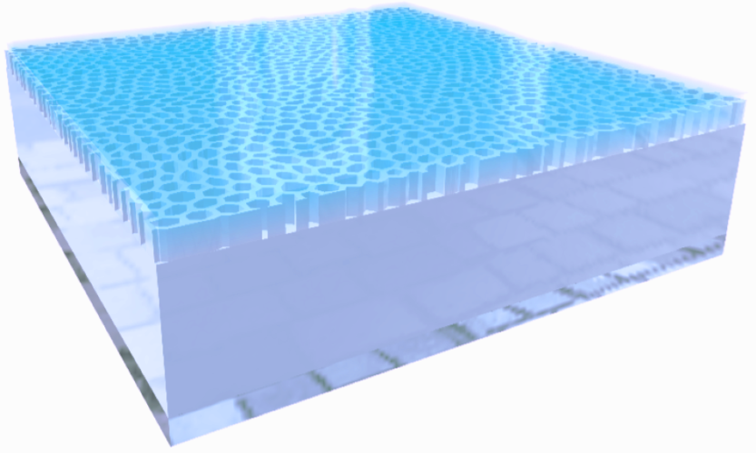
Co-led by Surrey University, the team’s 1μm thick solar panels convert light into electricity more efficiently than others and could pave the way to make it easier to general more clean, green energy.
In a paper published in Photonics, the team detail how they used characteristics of sunlight to design a disordered honeycomb layer which lies on top of a wafer of silicon. The honeycomb design enables light absorption from any angle and traps light inside the solar cell, enabling more energy to be generated.
In a statement, Dr Marian Florescu from Surrey University’s Advanced Technology Institute (ATI) said: “One of the challenges of working with silicon is that nearly a third of light bounces straight off it without being absorbed and the energy harnessed. A textured layer across the silicon helps tackle this and our disordered, yet hyperuniform, honeycomb design is particularly successful.”
Register now to continue reading
Thanks for visiting The Engineer. You’ve now reached your monthly limit of news stories. Register for free to unlock unlimited access to all of our news coverage, as well as premium content including opinion, in-depth features and special reports.
Benefits of registering
-
In-depth insights and coverage of key emerging trends
-
Unrestricted access to special reports throughout the year
-
Daily technology news delivered straight to your inbox


National Gas receives funding to develop Gravitricity underground hydrogen storage system
One single rock salt mine - Winsford - has 23 <i>MILLION </i>cubic metres of void and even allowing for 10% of that void set aside for hazardous waste...