"Superlattices" of 2D materials hold promise for new electronic devices
Technique for combining multiple layers of 2D materials with different properties can create tailored materials for computing and light-based technologies
Since the discovery of graphene, engineers have become more familiar with the properties of ultra-thin, two-dimensional materials. But the potential applications for these materials have so far depended on the properties of only homogeneous stacks of these layers. Chemists and materials scientists at the University of California Los Angeles (UCLA) have developed a technique for forming “superlattices” consisting of layers of dissimilar materials. These substances could form the basis for superfast and ultra-efficient transistors in microprocessors, and advanced LEDs and lasers, they claim.
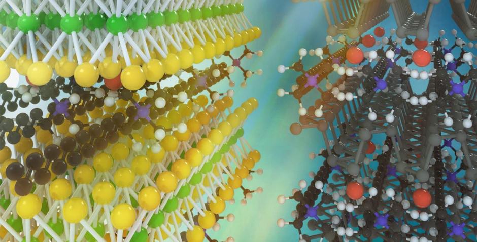
The key to these tailored properties is that unlike current superlattices, where adjacent layers must have very similar atomic structures and therefore electronic properties, the new technique allows radically different structures, properties and functions to be placed next to each other, but without interfering with each other. For example, one layer could allow fast transport of electrons through or across it, while the next layer could be an insulator.
Register now to continue reading
Thanks for visiting The Engineer. You’ve now reached your monthly limit of news stories. Register for free to unlock unlimited access to all of our news coverage, as well as premium content including opinion, in-depth features and special reports.
Benefits of registering
-
In-depth insights and coverage of key emerging trends
-
Unrestricted access to special reports throughout the year
-
Daily technology news delivered straight to your inbox


Water Sector Talent Exodus Could Cripple The Sector
Maybe if things are essential for the running of a country and we want to pay a fair price we should be running these utilities on a not for profit...