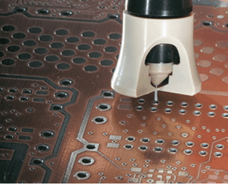
As electronic devices get smaller and smaller, ever more conducting paths must be positioned ever more closely together on printed circuit boards (PCBs). This is why, today, most PCBs are multilayered.
In order to transfer electronic signals through to all the layers, these are connected by plated through-holes, also called vias (vertical interconnect access), which are electroplated with an electrically conductive material such as copper.
To ensure proper function, the hole lining must be uniform. For quality control purposes, the thickness of the copper coating lining the through-hole is measured using the eddy current method: A specially designed probe tip, housing a tiny eddy current coil, is simply inserted into the through-hole.


Water Sector Talent Exodus Could Cripple The Sector
Maybe if things are essential for the running of a country and we want to pay a fair price we should be running these utilities on a not for profit...