The discovery of a method for growing semiconducting ribbons of graphene on a conventional substrate for electronics manufacture could lead to faster development of a new generation of electronics with enhanced capabilities in speed and performance, according to its developers at The University of Wisconsin-Madison. The technique should be easily scalable for mass production and is compatible with techniques already used in the electronics industry, the team claims.
One of the biggest barriers to the widespread use of graphene is the difficulty of making the material in a suitable form in a way that is controllable and repeatable. To be used in electronics, taking advantage of the materials excellent conductivity and ability to dissipate heat, graphene has to be in a form where current through it can be switched on and off; this entails producing strips of grapheme 10nm wide with a well-defined edge where carbon-carbon bonds are parallel to the edge (this is known as an ‘armchair’ edge).
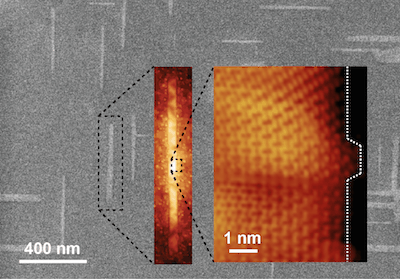
This has proved very difficult. Cutting a larger sheet into thin strips leaves rough edges; while growing nanoribbons has only been achieved on metal surfaces, and this has never yielded ribbons long enough to be useful.
The Madison team adopted the growing method, and used as their substrate wafers of germanium, a semiconductor widely used in electronics. The technique, which is described in a paper in Nature Communications, employs chemical vapour deposition, bathing the surface of the wafer in methane, which adsorbs onto the surface and then breaks down into hydrocarbon that react to form graphene.
The key to forming the long regular nanoribbons is to slow the process down by using very small vapour concentrations of methane. This forces the grapheme to grow on one specific crystallographic facet of the germanium’s atomic lattice structure.
“What we’ve discovered is that when graphene grows on germanium, it naturally forms nanoribbons with these very smooth, armchair edges,” said research leader Michael Arnold. “The widths can be very, very narrow and the lengths of the ribbons can be very long, so all the desirable features we want in graphene nanoribbons are happening automatically with this technique.”
Currently, the team is working on controlling where on the wafer the ribbons start growing and in which direction; at the moment the starting point is random and the ribbons can be oriented in two directions.
Graphene nanoribbons could be used in hybrid integrated circuits which would have faster processing speeds than conventional electronics, and in highly specific chemical and biological sensors and optical computing applications.
“Graphene nanoribbons that can be grown directly on the surface of a semiconductor like germanium are more compatible with planar processing that’s used in the semiconductor industry, and so there would be less of a barrier to integrating these really excellent materials into electronics in the future,” Arnold said in a statement.


Virgin Atlantic’s Flight100 saved 95 tonnes of CO2 in first SAF flight
LOL a time-honoured unit of volume measurement,, just as large <i>AREAS</i> are expressed as multiples of the size of Wales … or renewable energy...