A new process for purifying silicon and making it into crystalline wafers could reduce the cost of solar cells by up to a fifth, according to the process’s developers at the Fraunhofer Institute for Solar Energy Research in Freiburg, southwest Germany. The method is far less wasteful of material than conventional wafer manufacture, and also uses less energy.
Solar cell production starts with impure silicon, which is melted down and reacted with chlorine, to produce a material called chlorosilane. When hydrogen comes into contact with chlorosilane, it’s converted into pure silicon. But conventionaly, this process creates chunks of amorphous silicon rather than the precisely-ordered crystals needed for photovoltaic cells. To make this, the amorphous lumps have to be crushed, melted at 1450°C and crystallised into ingots weighing upwards of 200kg, which have to be sawn into wafers. The repeated heating uses a large amount of energy, and the sawing means that up to half of the silicon produced is lost as dust.
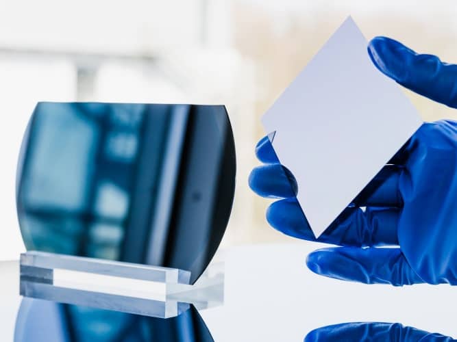
The first three stages of the new process are the same: melt the impure silicon, form chlorosilane then mix it with hydrogen. But rather than making amorphous silicon as an intermediate, the vapour-phase silicon from the hydrogen reaction is induced to flow past a crystalline silicon wafer, and as the gas covers the wafer surface, the silicon atoms on its surface act as a template for crystalline growth. A porous silicon layer acts as a mechanical breakpoint, allowing the newly-deposited silicon layer to be detached from the substrate as a fresh crystalline wafer; the substrate can be reused several times. “In this way we get a very good monocrystal, which is the best type of crystal, and the wafers are of the same quality as those produced using conventional methods,” says lead researcher Stephan Janz. “With our method, we can avoid almost all of the losses that occur during the conventional production process.” he added. “This means we are reducing material losses by 50 per cent while using 80 per cent less energy.”
The process also allows the production of wafers of predefined thickness with no need for sawing. Conventionally, wafers must be 150–200µm thick, to avoid losses from mechanical cutting; but for PV applications, thinner cells work just as well and are cheaper. Cutting material costs by half reduces the cost of the final fabricated cell by 20 per cent, according to the researchers.
The team has set up a company called NexWafe to commercialise the process: a factory to produce wafers is expected to be able to start mass production in late 2017.


Poll: Should the UK’s railways be renationalised?
I _do_ remember British Rail - and that it was <i>literally</i> a national joke https://youtu.be/zV2lmSDKvO8