
Part 1
Richard Anslow and Dara O’Sullivan
Analog Devices, Inc.
Condition-Based Monitoring Is Essential for Realising Industry 4.0.
Government initiatives, such as Germany’s Industrie 4.0 and China’s Made in China 2025, are accelerating the trend towards ubiquitous networked automation in manufacturing. In addition, automation is being enhanced by smart sensor systems with more data available to monitor and control production processes. In particular, Made in China 2025 aims to rapidly develop high tech industries, including electric vehicles, next-generation information technology (IT) and telecommunications, and advanced robotics and artificial intelligence. With more advanced systems there is a need for more advanced ways to ensure system reliability.
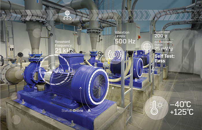
Condition-based monitoring (CbM) of robotics and rotating machines, such as turbines, fans, pumps, and motors, records real-time data related to the health and performance of the machine to enable targeted predictive maintenance, as well as optimized control. Targeted predictive maintenance, early in the machine life cycle, reduces the risk of production downtime resulting in increased reliability, significant cost savings, and increased productivity on the factory floor.
How to Implement a Wired Condition-Based Monitoring Solution?
Condition-based monitoring of industrial machines can utilize a range of sensor data, such as electrical measurements, vibration, temperature, oil quality, acoustic, and process measurements such as flow and pressure. However, vibration measurement is the most common by far, as it can provide the most reliable indication of mechanical issues such as imbalance and bearing failure. This article focuses on the use of vibration sensing, but the methodology is equally applicable to data from other sensors.
The transmission means of the sensor data from the sensing node to the main controller or the cloud is highly dependent on applications. In many applications, some local data processing is implemented at the edge node, with summary data being subsequently transmitted wirelessly to anetwork gateway, or directly via a cellular link to the cloud or analytics server. In these situations, the amounts of data transmitted are typically rather low, and there is often a requirement for low power as the edge node can be battery powered. In other applications, raw sensor data transmission is required. For example, aligning and fusing data from multiple sensors may be required prior to analysis. Raw data transmission is also required in applications where data is utilized for real-time control. In these applications, a wired interface is a more likely solution for data transmission.
CbM of industrial applications can leverage Analog Devices’ optimized signal chain of microelectricalmechanical systems (MEMS)accelerometers, low power microcontrollers, and wired iCoupler® isolated interfaces to extract, condition, and reliably communicate machine health data from a remote CbM slave back to a master controller for analysis. Over time, machine health data can be used to create software-based models to determine changes in machine behavior and proactively maintain machine health. In some applications, such as CNC machines, the data can also be used to optimize the performance of the system in real time.
The challenges with implementing a wired CbM interface include EMC robustness when operating over long cables, data integrity with transmitting at ahigh baud rate (for real-time CbM data streaming), and communication physical layer/protocol mismatches. Analog Devices’ signal chain and system-level expertise provides several possible options to implement a wired CbM interface.
This article (part 1 of 2) presents Analog Devices’ wired interface solutions, which reduce customer design cycle and test time, and enable faster time to market for industrial CbM solutions. The next article will focus on detailed physical layer design considerations, at both the master controllerand the wired CbM slave.
Wired CbM Design Implementation
Designing and deploying a wired condition-based monitoring solution requires several system performance considerations and trade-offs.
Firstly, when selecting a suitable MEMS accelerometer, the type of fault that requires measurement must be considered so that the correct bandwidth and noise performance MEMS can be chosen to meet system requirements. Edge node processing requires careful matching of the selected processor to ensure maximum system flexibility.
Secondly, the design of a wired CbM system requires careful selection of a suitable wired communication protocol and physical layer to enablehigh speed real-time data streaming. Implementing a wired interface requires careful consideration of EMC performance, data transmissioncabling, connectors, and power delivery over the cabling.
Selecting a Suitable MEMS Accelerometer
Selection of a suitable MEMS vibration sensor has multiple aspects:
Number of Axes
The number of axes being monitored is usually a function of the fault type and the sensor mounting arrangement. If the fault has a clearly dominantaxis,
and a clear transmission path in that axis, then a single axis sensor may be sufficient. Three-axis sensing is useful for faults that contain energy inmultiple axes or indeed where the transmission path of the fault energy is unclear.
Types of Faults
The type of fault being monitored has a significant impact on the sensor choice. Sensor noise density and bandwidth are important specifications in this regard as they determine the vibration level and frequency range that can be reliably extracted. As an example, imbalance and misalignment fault for low rotation rate machines may require a low noise density sensor, but bandwidth requirements are fairly low, while gear fault detection can require both low noise density and high bandwidth specifications in the sensor.
Performance Requirements
Along with the fault type, the performance requirement of the CbM is important to understand. Alarm detection for basic traffic light-type condition indicators requires a different level of performance for sophisticated prognostics. This clearly applies to the analytics and algorithms being deployed, but also has an impact on the sensor choice. The higher the performance level of the sensor in terms of bandwidth, noise density, and linearity, the more advanced the analytics capability will be.
Selecting Suitable Signal Processing
Design considerations include:
Accelerometer Output
The output of the accelerometer is typically either analog or serial digital signaling, typically SPI. An analog output sensor will require a conversionstage to digital, as well as some signal conditioning. This could be a discrete ADC with preamplifier conditioning, or an embedded ADC in amicrocontroller.
Edge Node Processing Requirements
Some basic FFT or signal processing algorithms may be required at the edge node in order to reduce the burden on the data link and/or the central controller/server.
Data Transmission Protocol Requirements
The output of the ADC or sensor is typically an SPI interface. This does not inherently provide any mechanisms for data integrity checking, time stamping, mixing data from different sensors, etc. It can be useful to encapsulate the sensor data in a higher level protocol at the edge node prior to transmission. This can add robustness and flexibility to the sensor interface, but adds a requirement at the edge node for handling and packaging the data stream appropriately.
For more information, please refer to the Analog Dialogue article “Choosing the Most Suitable MEMS Accelerometer for Your Application.”
Porting Accelerometer Output to a Wired Communication Bus
As previously noted, the output of the accelerometer is typically either analog or serial digital signaling, typically SPI. The SPI output can either be locally processed (allowing protocol flexibility) and then added to the physical layer interface, or directly ported to the physical layer.
SPI is an unbalanced single-ended serial interface, intended for short distance communication. To directly port SPI to the physical layer over longerdistances, RS-485 line drivers and receivers can be used. RS-485 signaling is balanced, differential, inherently noise immune, and robust over long cablelengths.
When using SPI over longer distances between an SPI master and slave, there are some challenges. SPI is synchronous in nature, with a clock (SCLK) initiated by the SPI master. The SPI data lines—master output slave input (MOSI) and master input slave output (MISO)—are synchronized to the SCLK, which is reliably achieved over short distances. SPI also has an active, low enable chip select (CS) signal, which allows individual slave addressing if required.
Over long cable runs, the SCLK signal will incur a propagation delay through the cable, of the order of 500 ns for a 100 m cable. For a MOSI datatransfer, the MOSI and SCLK are equally delayed by the cable. However, data sent from the slave MISO to the master will be out of sync by twice the cable propagation delay.
To restore synchronicity between the master and slave, one can either feed the clock signal from the slave back to the master or compensate for cable delay in the master microcontroller using a clock phase shift. The phase shift of the clock must match the total delay of the system. AN-1397 provides implementation details for a master microcontroller delay compensation.
Wired Communication Physical Layer
When communicating over long distances, a robust physical layer is required. As previously noted, RS-485 signaling is balanced, differential, and inherently noise immune. System noise couples equally to each wire in an RS-485 twisted pair cable. One signal emits theopposite of the other signal, and electromagnetic fields coupled onto the RS-485 bus cancel each other out. This reduces the electromagneticinterference (EMI) of the system. Some additional key benefits that make the RS-485 ideal for CbM systems include:
- Higher data rates, up to 50 Mbps on shorter cable lengths (less than 100 m)
- Use of cable lengths up to 1000 m at lower data rates
- Full-/half-duplex RS-485 and RS-422 multiple driver/receiver pairs can translate bidirectional SPI to RS-485 bus signals using minimum component count
- Wide common mode input range allows for differences in ground potential between master and slave
EMC Performance of the Wired Interface
Over long cable runs, communication networks can be subject to hazards like large common-mode noise, ground potential differences, and high voltage transients.
Conducted and radiated noise sources can affect communication reliability along 100 m cable lengths. Immunity to these noise sources can beincreased by using Analog Devices’ iCoupler chip scale transformer isolation technology. AN-1398 provides a summary of immunity to common industrial transients achieved using iCoupler technology.
Common-mode transient immunity (CMTI) is the ability of an isolator to reject high voltage/high slew rate noise transients and maintain error free communication. Signal and isoPower® isolated devices offer a minimum common-mode transient immunity of 25 kV/μs, and can also withstand up to a maximum of 100 kV/μs without permanent latch up or damage.
In factory automation environments, system designers often don’t have control over the electrical installation supplying their communication network. It is best practice to assume that ground potential differences exist. In motion control systems, ground potential differences ofhundreds of volts can occur. An RS-485 communication node requires galvanically isolated power and data lines to operate reliably in these environments. Signal and isoPower isolated devices offer a maximum continuous working voltage of 600 V peak (basic) or 353 V peak (reinforced). The basic insulation enables reliable communication in the presence of large ground potential differences. The reinforced insulation protects operators from electric shock events on the factory floor.
In a wired communication network, the exposed connectors and cabling can be exposed to a number of harsh high voltage transients. The system level IEC 61800-3 standard relating to EMC immunity requirements for adjustable speed, electrical power drive systems require aminimum ±4 kV contact/±8 kV air IEC 61000-4-2 ESD protection. Analog Devices’ next-generation RS-485 transceivers offer greater than ±8 kVcontact/±8 kV air IEC 61000-4-2 ESD protection.
Phantom Power over Data Lines
Distribution of both power and data lines between master controllers and remote CbM sensor nodes requires innovative solutions to reduce cable costs. Combining both data and power on a single-twisted pair means significant system cost savings, as well as enabling smaller printed circuit board (PCB) connector solutions at space constrained edge sensor nodes.
Power and data are distributed on a twisted pair using an inductor-capacitor network. High frequency data is coupled to the data lines through series capacitors, which also protect the RS-485 transceiver from dc bus voltages. A power supply is connected at the master controller via an inductor connected to a data line, and the power is then filtered out using an inductor at the CbM slave sensor node at the far end of the cable.
The inductances at both ends of the cable should be well matched to avoid differential mode noise and self-resonance frequency should be at least 10 MHz to avoid interference with the real-time burst mode of Analog Devices’ next-generation vibration measurement systems. Note that the power and data coupling solution must be added to a data line where dc data content is not expected, such as MOSI or MISO to RS-485 extensions.
Recommended Solutions and Performance Trade-Offs
Based on the design considerations presented, the following components provide optimal paths to robust wired industrial vibration measurement solutions.
- ADcmXL3021, wide bandwidth, low noise, triaxial vibration sensor
- ADuM5401/ADuM5402, quad-channel, 2.5 kV isolators with integrated dc-to-dc converter
- ADM3066E, 50 Mbps half duplex RS-485 transceiver
- ADM4168E, 30 Mbps dual RS-422 transceiver
- LTC2858-1, 20 Mbps full duplex RS-485 transceiver
- ADP7104, 20 V, 500 mA, low noise, CMOS LDO regulator
Recommended Solutions
The ADcmXL3021 MEMS accelerometer is common to all three solutions. This accelerometer features ultralow noise density (25 µg/√Hz), which supports excellent resolution. The ADcmXL3021 also has a wide bandwidth (dc to 10 kHz with 5% flatness), which enables tracking of key vibrationsignatures on many machine platforms. The ADcmXL3021 offers the customer a mechanically optimized aluminum package, which provides consistent coupling to the integrated MEMs sensors over a broad frequency range. This ensures that the vibration signature from the measured equipment is reliably extracted and conditioned.
The ADcmXL3021 is available with SPI output, which can be interfaced directly to the RS-485/RS-422 devices, or indirectly via microprocessor and/or iCoupler signal and power isolation to the RS-485/RS-422 devices, as shown in Figure 1. For real-time monitoring of vibration signatures on industrial equipment, the ADcmXL3021 includes a real-time streaming mode, which operates at approximately 12 Mbps SPI.
To interface the real-time streaming SPI mode to an RS-485 bus, components with significant data rate capabilities must be chosen. The ADM3066E/ADM4168E/LTC2858-1 RS-485/RS-422 transceivers all operate at 20 Mbps data rates and above.
For Option 1 and Option 2 shown in Figure 1, with direct SPI to RS-485 connections, the ADM3066E and ADM4168E provide a robust interface to implement an SPI 3 receive, 1 transmit (3+1) configuration for a slave vibration sensor node. The SPI CS receive signal is implemented usingthe ADM3066E, and the SPI CLK, MOSI, and MISO signals are implemented using the ADM4168E. When operating in real-time streaming mode, the ADcmXL3021 sends an interrupt signal to the master microcontroller to flag when a new data burst is available for capture. The interrupt signal (/BUSY) can also be transmitted to the master using the ADM4168E.
The complete solution consists of three signals sent from the master to the ADcmXL3021 (MOSI, CS, CLK), and two signals sent from the ADcmXL3021 back to the master (MISO, /BUSY). The 5× single-ended signals can be translated to differential signaling using just two components—the ADM4168E and ADM3066E. The differential signals can be accommodated using RJ50 connectors and plugs, which consume almost identical PCB area when compared to industry standard RJ45 Ethernet connectors. The ADM3066E and ADM4168E transceivers offer greater than ±8 kV contact/±8 kV air IEC 61000-4-2 ESD protection, which offers essential robustness when directly connected to a wired cable interface.
For Option 3, the microcontroller allows preprocessing of the ADcmXL3021 SPI output, as well as the possibility to perform a protocol translationbetween SPI and other serial interfaces, such as UART. UART is a commonly used asynchronous protocol with RS-485 interfaces. The UART consists of transmit and receive signals, as well as a transmit enable signal, all of which can be wired directly to a full-duplex RS-485 transceiver, such as the LTC2858-1. The LTC2858-1, in full-duplex mode, allows simultaneous bidirectional data transfer, matching the requirement for SPIbidirectional data transfers. The microcontroller can handle the synchronous SPI to asynchronous UART protocol translation.
The ADuM5401/ADum5402 are the industry’s smallest form factor signal and power isolated devices. They include an integrated dc-to-dc converter, which provides up to 500 mW of regulated, isolated power at either 5.0 V or 3.3 V from a 5.0 V input supply.
In Figure 1, Option 2 includes the ADuM5401, which takes 5 V dc from the data bus and provides 3 V isolated power to the ADcmXL3021. The ADuM5401 also includes 4 channels of signal isolation, in a configuration suitable for 3+1 SPI isolation.
Option 3 in Figure 1 contains the ADuM5402, which is similar to the ADuM5401. The key difference is that the ADuM5402 provides 2 transmit and 2 receive digital isolation channels.
As previously mentioned, the ADuM5401/ADuM5402 add increased EMC immunity to the wired CbM interface, protecting the ADcmXL3021 from high voltage disturbances and ground potential differences on the RS-485 cabled interface.
Performance Trade-Offs
Table 1 compares the three solutions using a number of key metrics including design flexibility, PCB area, solution cost, complexity, and EMC performance.
Integrating a microcontroller at the CbM sensor node will allow increased design flexibility, but at the expense of increased PCB area and additional software complexity. As the master CbM node will have a processor, this means that Option 3 in Figure 1 will essentially be a two microcontroller system, which will be slower to get up and running compared to a single microcontroller at the master CbM node.
Option 1 and Option 2 provide low design flexibility, but a path to more rapid deployment as they can facilitate low complexity, transparent SPI to RS-485 links. Option 1 and Option 2 also provide a path to smaller PCB form factor compared to Option 3, which would require additional PCB area for the microcontroller and associated circuitry (for example, a clock oscillator and several passive components).
Adding iCoupler signal and power isolation to Option 2 and Option 3 incurs a minimal PCB area penalty, and boosts EMC performance beyondwhat is achieved using on-chip protection with the RS-485/RS-422 transceivers.
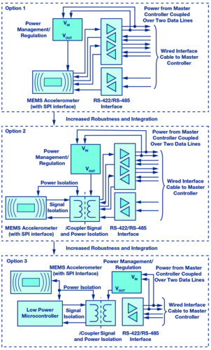
Figure 1. Options for a robust, highly integrated, wired MEMS accelerometer condition-based monitoring solution.
Table 1. Trade-Off Comparison Between CbM Options
| Solution Option | Design Flexibility | PCB Area | Solution Cost | Complexity/ Integration | EMC Performance |
| 1 | Low | Low | Low | Low | Medium |
| 2 | Low | Low/ medium | Low/ medium | Low | High |
| 3 | High | Medium | Medium | Medium | High |
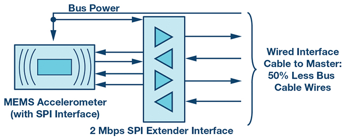
Figure 2. LTC4332 SPI extender interface saves cable costs.
Lower Data Rate Solutions
For wired applications running at lower data rates (less than 2 Mbps) the LTC4332 SPI extender offers an alternative implementation forruggedizing a SPI link between a master and remote slave sensor node. The LTC4332 can transmit SPI data, including an interrupt signal over two twisted pair cables. This solution provides significant cost savings, as up to 50% less bus cabling can be used compared to standard solutions.
About the Authors
Richard Anslow is a systems applications engineer with the Connected Motion and Robotics Team within the Automation and Energy business unit at Analog Devices. His areas of expertise are condition-based monitoring and industrial communication design. He received his B.Eng. and M.Eng.degrees from the University of Limerick, Limerick, Ireland. He can be reached at richard.anslow@analog.com.
Dara O’Sullivan is a system applications manager with the Connected Motion and Robotics Team within the Automation and Energy business unit at Analog Devices. His area of expertise is power conversion, control, and monitoring in industrial motion control applications. He received his B.E., M.Eng.Sc., and Ph.D. degrees from University College Cork, Ireland, and has worked in industrial and renewable energy applications in a range of research, consultancy, and industry positions since 2001. He can be reached at dara.osullivan@analog.com.


Water Sector Talent Exodus Could Cripple The Sector
Maybe if things are essential for the running of a country and we want to pay a fair price we should be running these utilities on a not for profit...