Richard Anslow, System Applications Engineer and
Dara O’Sullivan, System Applications Engineer
Introduction
In the first part of this article, “Enabling Robust Wired Condition-Based Monitoring for Industry 4.0—Part 1,” we presented Analog Devices’ wired interface solutions, which reduce customer design cycle and test time, and enable faster time to market for industrial CbM solutions. Several aspects were discussed, including selecting a suitable MEMS accelerometer and physical layer, as well as EMC performance and power design. In addition, three design solutions and performance trade-offs were presented in Part 1. This article (Part 2 of 2) focuses on detailed physical layer designconsiderations for the SPI to RS-485/RS-422 design solutions presented in Part 1.
Common challenges in implementing a wired physical layer interface for MEMS include managing EMC robustness and data integrity. However, when extending a clock synchronized interface such as SPI over long RS-485/RS-422 cables, along with combining power and data on the sametwisted pair wires (phantom power), several additional challenges are presented. This article discusses the following key considerations andprovides recommendations for designing the physical layer interface:
- Managing system time synchronization
- Data rate vs. cable length recommendations
- Filter design and simulation for shared power and data architectures
- Passive component performance trade-offs for phantom power implementation
- Component selection and system design window
- Experimental measurements
Time Synchronization and Cable Length
When designing an SPI to RS-485/RS-422 link, the cable and components affect system clock and data synchronization. Over a long cable run, the SCLK signal will incur a propagation delay through the cable, approximately 400 ns to 500 ns for a 100 m cable. For a MOSI data transfer, the MOSIand SCLK are equally delayed by the cable. However, data sent from the slave MISO to the master will be out of sync with the SCLK by twice the cable propagation delay. The maximum possible SPI SCLK is set by the system propagation delay, which includes cable propagation delay as well as master and slave component propagation delays.
Figure 1 illustrates how system propagation delay can lead to inaccurate SPI MISO sampling at the SPI master. For a system without an RS-485/RS-422 cable, MISO data and SPI SCLK will be synchronized with little or no delay. For a system with a cable, MISO data at the SPI slave is out of sync with SPI SCLK by one system propagation delay, noted as tpd1 in Figure 1. MISO data arrives back at the master out of sync by twosystem propagation delays, noted as tpd2. As data is shifted right due to cable and component propagation delays, inaccurate data samplingoccurs.
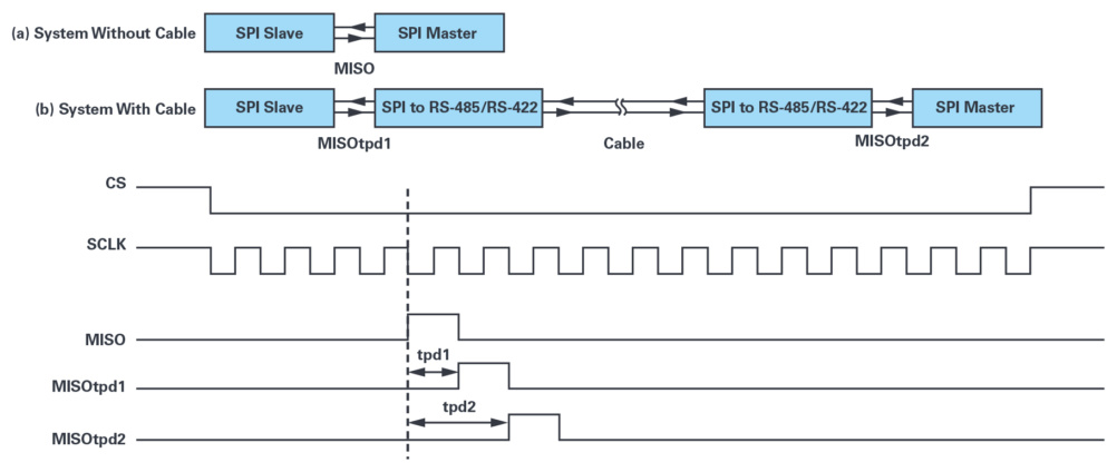
Figure 1. Synchronization of MISO data and SPI SCLK for a system with and without a long RS-485/RS-422 cable.
To prevent inaccurate MISO sampling, one may reduce the cable length, lower the SPI SCLK, or implement an SPI SCLK compensation scheme (clockphase shift) in the master controller. Theoretically, the system propagation delay should be less than 50% of the SCLK clock period for error freecommunication, and in practice a limit of system delay of 40% SCLK can be used as a general rule.
Figure 2 provides an SPI SCLK vs. cable length guideline for the two SPI to RS-485/RS-422 designs described in Part 1.1 The nonisolated design uses Analog Devices’ high speed EMC robust and small form factor RS-485/RS-422 devices (ADM3066E and ADM4168E). The isolated design also includes Analog Devices’ iCoupler® signal and power isolated ADuM5401 device, which provides additional EMC robustness and noise immunity for SPI to RS-485/RS-422 links. This design adds additional system propagation delay, which limits operation at higher SPI SCLK rates. Over longer cable runs (greater than 30 m) adding isolation is strongly recommended to help mitigate against ground loops and EMC events such as electrostatic discharge (ESD), electrical fast transients (EFT), and high voltage surges coupling to the data transmission cabling. When cable lengths extend to 30 m or greater, the SPI SCLK vs. cable length performance of the isolated vs. nonisolated design is similar, as illustrated in Figure 2.
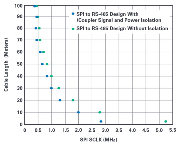
Figure 2. SPI SCLK vs. cable length guidelines for isolated and nonisolated designs.
Phantom Power
Background
Phantom power combines power and data on a single twisted pair—enabling a 1-cable solution between master and slave devices. Combining both data and power on a single cable enables a 1-connector solution at space constrained edge sensor nodes.
Power and data are distributed on a single twisted pair using an inductor capacitor network, as shown in Figure 3. High frequency data is coupled tothe data lines through series capacitors, which also protect the RS-485/RS-422 transceiver from dc bus voltages, as shown in Figure 3a. Figure 3 shows a power supply connected at the master controller via an inductor connected to a data line. The 5 V dc power biases the ac data bus as illustrated in Figure 3b. In Figure 3c the current path is shown as IPWR between the master and slave, with the power extracted from the line using an inductor at the condition-based monitoring (CbM) slave sensor node at the far end of the cable.
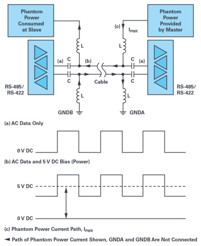
Figure 3. Phantom power physical layer ac and dc voltage levels.
High-Pass Filter
For the purposes of this article, it is assumed that the phantom power inductor-capacitor network is added to two wires, which route the RS-485/RS-422 conversion of the SPI MISO signal. Figure 4 illustrates the master and slave SPI to RS-485/RS-422 design and the phantom power filtercircuit for the SPI MISO data line. The filter circuit is high pass, and thus requires that the data signals being transmitted do not have content at dc orat very low frequencies.
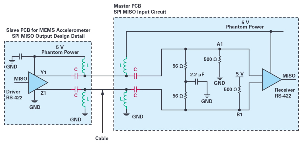
Figure 4. SPI to RS-485/RS-422 design and phantom power filter circuit.
A second-order high-pass filter circuit is shown in Figure 5, which is a simplified representation of Figure 4. The voltage output at the transmitting RS-485/RS-422 device is noted as VTX , with R1 15 Ω output impedance. The R2 30 kΩ is a standard input impedance for the receiving RS-485/RS-422 device. Inductor (L) and capacitor (C) values can be selected to suit the desired system data rate.
When choosing the inductor (L) and capacitor (C) values, the maximum RS-485/RS-422 bus voltage droop and droop time need to be considered, as illustrated in Figure 6. Standards exist, such as single twisted-pair Ethernet,2 which specify the maximum allowable voltage droop and droop time as shown in Figure 6a. For some systems the maximum permissible voltage droop and droop time may be larger, limited by the signal polarity crossover point, as shown in Figure 6b.
The voltage droop and droop time can be used paired with a simulation of Figure 5 to determine the system high pass frequency.
For a well damped system, the relationship between the high-pass filter cutoff frequency and the droop requirement is given by Equation 1.3
When adding phantom power to an SPI to RS-485/RS-422 communication system it is clear that the minimum possible SPI SCLK rate will be limited by the phantom power filter components.
To achieve reliable communication without bit errors, one needs to consider the minimum SPI SCLK in a worst-case scenario—for example, where all SPI MISO sampled bits are logic high, as illustrated in Figure 7. If all sampled MISO bits are logic high, then this results in a bit rate lower than thesystem SPI SCLK. For example, if the SPI SCLK is 2 MHz and all 16 bits are logic high, then the phantom power LC filter network will see anequivalent SPI MISO bit rate of 125 kHz.
As noted in the section “Time Synchronization and Cable Length,” longer cable lengths require lower SPI SCLK rates. However, phantom power limits the lowest possible SPI SCLK rate. Balancing these opposing requirements involves careful selection and characterization of passive filter components, particularly inductors.
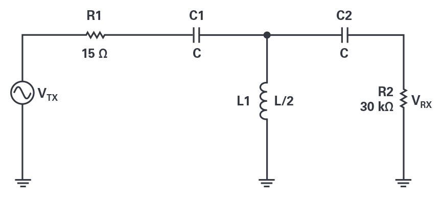
Figure 5. Second-order high-pass filter for RS-422 transmit and RS-485/RS-422 receive data path.
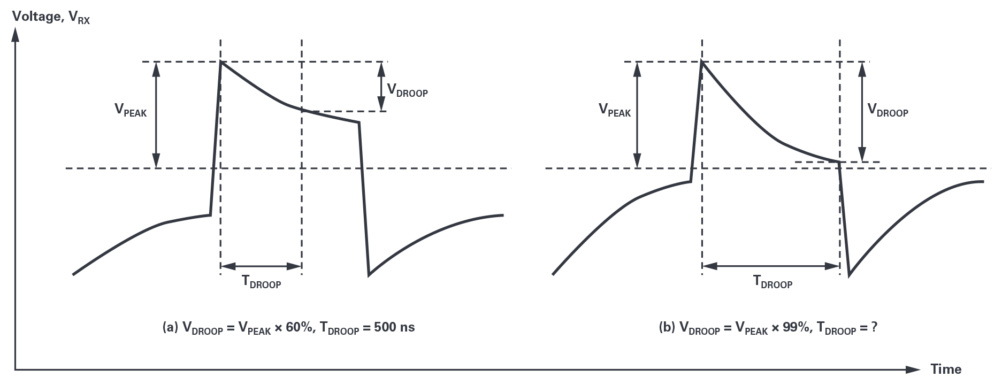
Figure 6. Voltage droop and droop time at RS-422 receiver.
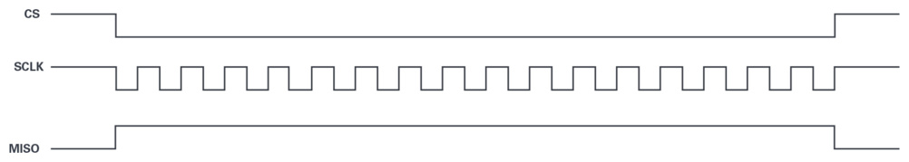
Figure 7. SPI protocol with MISO 16-bit burst, all logic high.
Passive Component Selection
When selecting a suitable power inductor, a number of parameters need to be considered, including sufficient inductance, rated/saturation current, self-resonant frequency (SRF), low dc resistance (DCR), and package size. Table 1 presents selected power inductors and parameters of interest.
The rated current needs to meet or exceed the total current requirements for the remotely powered MEMS sensor node, and the rated saturation current needs to be much larger.
The inductor will not present a high impedance to ac data above its quoted SRF, and at a certain point will begin to have a capacitive impedancecharacteristic. The chosen inductor SRF will limit the maximum SPI SCLK that can be used on the SPI to RS-485/RS-422 physical layer, as shown inTable 1. When operating over long cables the inductor SRF may not be reached; for example, reaching SPI SCLK rates of 11 MHz (part number 744043101’s SRF) over 10 m of cable may not be possible. In other cases, when operating over long cables the inductor SRF may be reached forlower SPI SCLK rates (2.4 MHz, 1.2 MHz). As noted previously, when used in a phantom power filter network, an inductor will also limit the lowest possible SCLK rate.
Larger inductor values are available in 12.7 mm × 12.7 mm packages, while smaller value inductors are available in 4.8 mm × 4.8 mm packages.
Table 2 shows that trading off opposing requirements to minimize inductor size is challenging due to physical constraints (internal windings).
Table 1. Power Inductor Parameters of Interest
| Part Number | L (µH) | IRATED (mA) | Self-Resonant | DC Resistance (DCR) | Package Size (mm) |
| 744043101 | 100 | 290 | 11 | 0.6 | 4.8 × 4.8 |
| LPS8045B-105 | 1000 | 230 | 1.3 | 3.22 | 8.0 × 8.0 |
| 76877530 | 1000 | 300 | 2.4 | 3.3 | 7.8 × 7.0 |
| SDR0805-102KL | 1000 | 210 | 3.0 | 4.5 | 7.8 × 7.8 |
| 7687714222 | 2200 | 260 | 1.2 | 6.5 | 10 × 10 |
| SRR1208-222KL | 2200 | 280 | 0.65 | 4.2 | 12.7 × 12.7 |
Table 2. Power Inductor—Constraints on Package Size
| Parameter | Implications for Package Size |
| Sufficiently High Inductance | Higher inductance values result in more internal windings and larger package size. |
| Higher SRF | Higher SRF will mean less internal windings and smaller size. |
| Higher Rated and Saturation Current | Less internal windings, but larger package size. |
| Low DCR | To achieve lower DCR, wires need to be thicker and have fewer windings. |
The constraints in choosing a suitable dc voltage blocking capacitor are limited to the transient overvoltage rating and dc voltage rating. The dc voltage rating needs to exceed the maximum bus voltage bias, as illustrated in Figure 3. During a cable or connector short, the inductor currents will become imbalanced and will be dissipated by termination resistances. DC blocking capacitors need to be rated for peak transient voltages in theevent of a short. For example, in lower power systems, with inductor saturation currents of about 1 A, the corresponding dc blocking capacitor should be rated to at least 50 V dc.4
System Implementation
Design Window and Component Selection
When extending a clock synchronized interface such as SPI over long RS-485/RS-422 cables, along with combining power and data on the same twisted pair wires (phantom power), Figure 8 summarizes the design constraints noted in this article. The minimum possible SPI SCLK is set by the phantom power filter components, which high-pass filter data on the SPI data line. The maximum SPI SCLK is set by either the phantom power inductor self-resonant frequency (SRF) or the system propagation delay (whichever SPI SCLK is lower in value).
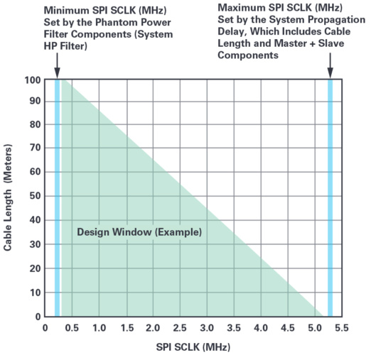
Figure 8. Design window constraints.
Table 3 provides suggested inductance and capacitance values, and the corresponding minimum SPI SCLK determined by simulating Figure 5 and using Figure 6 and Equation 1 for guidance. This assumes that VDROOP is 99% of VPEAK. This minimum SPI SCLK also considers the worst-case scenario, as described in Figure 7, where all bits in a data burst are logic high. The corresponding cable length is estimated using Figure 2. Themaximum SPI SCLK is set by either the system propagation delay or the inductor SRF value.
The following is an example calculation.
To determine the maximum SPI SCLK:
- Specify the required cable length for the system. For this example, we will choose 10 m of RS-485/RS-422 cable.
- Use Figure 2 to determine the maximum possible SPI SCLK for the system. For 10 m of cable, this is about 6 MHz SPI SCLK. Derating themaximum SPI SCLK by 10% to allow for LC component tolerances provides an SPI SCLK of 2.3 MHz. The maximum possible SPI SCLK may also belimited by the SRF of the chosen inductor.
To determine the minimum SPI SCLK:
- Consider an SPI protocol where all bits on the MISO line are logic high. For this example we will choose a 16-bit SPI protocol, where 16 bits of SPI MISO data will be sampled during 32 SCLK transitions. If all 16 bits are logic high, then the effective bit rate is 2.3 MHz / 32 = 72 kHz.
- Using Figure 5 with a 72 kHz square wave on VTX, the voltage waveform at the far end of the cable VRX can be simulated for a variety of L and C values. As cable length increases, the inductor value and inductor package size increase. The capacitance value also increases.
- The selection of L and C values is subjective and depends on the desired droop settings as described in Figure 6. For this example, we will assume that VDROOP = VPEAK × 99%.
- Using 100 µH inductors and 3.3 µF capacitors and a 72 kHz square wave on VTX yields a TDROOP of 7 µs, where VDROOP = VPEAK × 99%.
- A TDROOP of 6 µs to 7 µs is equivalent to 2.3 MHz to 2.6 MHz SPI SCLK.
- If choosing a 100 µH (744043101) inductor, an SPI SCLK of 6 MHz is lower than the inductor SRF of 11 MHz.
If 100 µH inductors and 3.3 µF capacitors are used, this results in the smallest component PCB area. When using larger inductors, such as 1000 µH or 2200 µH, the component PCB area can increase by a factor of three. The theoretical maximum SPI SCLK is set by the inductor SRF, which in practice may not be possible—for example, at 11 MHz using the 100 µH (744043101) in a system without clock compensation.
Table 3. Varying Phantom Power Filter Components
| L (µH) and Part Number | C (µF) | Max SPI SCLK (MHz) | Max SPI SCLK Set By | Min SPI SCLK | Max RS-485/RS-422Cable Length (m) |
| 100 | 3.3 | 5.2 | System propagation delay | 2.6 MHz | 10 |
| 1000 | 4.7 | 2.4 | Inductor SRF | 700 kHz | 60 |
| 2200 | 10 | 1.2 | Inductor SRF | 350 kHz | >100 |
If using larger inductors, such as 2200 µH, additional capacitance and resistance is needed in the network to damp system resonances. The additional components are colored blue and noted as RDAMP (1 kΩ) and CDAMP (47 µF) in Figure 9.
Experimental Setup
Figure 10 shows Analog Devices’ wired CbM evaluation platform, hereafter referred to as Pioneer 1. This system uses the SPI to RS-485/RS-422design solutions presented in Part 1 of this article. Pioneer 1 also includes the ADcmXL3021 wide bandwidth, low noise, triaxial MEMS accelerometer, which combines high performance with a variety of signal processing to simplify the development of smart sensor nodes in CbM systems. The SPI to RS-485/RS-422 slave extends the ADcmXL3021 SPI output over 10 m back to the master controller for vibration data analysis. The SPI to RS-485 designs use phantom power 100 µH inductors and 3.3 µF capacitors to minimize the size of the slave interface solutions, which measure 26 mm × 28 mm (excluding interface connector).
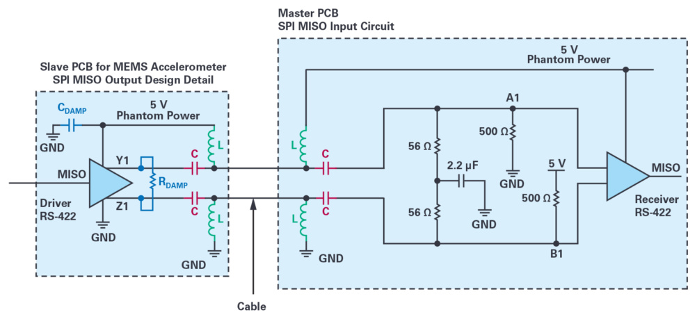
Figure 9. Adding additional system damping for larger inductance and capacitance filters.
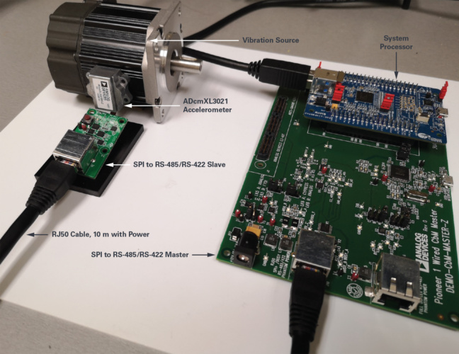
Figure 10. Pioneer 1 wired condition-based monitoring evaluation system.
AC Data Waveforms on Phantom Power Wires
Figure 11 and Table 4 describe the voltages measured at the SPI master and slave, and on the RS-485/RS-422 differential voltage bus. These voltages were measured using the sample application setup in Figure 10. The analog signals 1 (yellow) and 2 (blue) are the differential bus voltage representation of the MISO signal (purple), as measured at the SPI slave output. The digital signal 4 (yellow) shows the MISO sampled at the master controller. The MISO signal at the SPI master matches the polarity and phase of the MISO at the SPI slave, with little propagation delay.
Table 4. Oscilloscope Channels and Signals Measured
| Parameter | Implications for Package Size |
| 2 Digital (red) | ADcmXL3021 BUSY measured at master |
| 3 Digital (orange) | ADcmXL3021 MOSI measured at master |
| 4 Digital (yellow) | ADcmXL3021 MISO measured at master |
| 5 Digital (green) | ADcmXL3021 SCLK measured at master |
| 6 Digital (blue) | ADcmXL3021 CS measured as master |
| 3 Analog (purple) | ADcmXL3021 MISO measured at slave |
| 2 Analog (blue) | RS-422 Z pin bus voltage state corresponding to MISO; Differential Y to Z corresponds to 3 Analog (purple) and 4 Digital (yellow) |
| 1 Analog (yellow) | RS-422 Y pin bus voltage state corresponding to MISO; Differential Y to Z corresponds to 3 Analog (purple) and 4 Digital (yellow) |
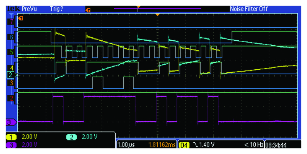
Figure 11. Voltages measured at the SPI master and slave, and on the RS-422 differential voltage bus.
DC Correctness on Phantom Power Wires
Figure 12 illustrates the ADcmXL3021 normal modes, which include an SPI protocol that sends 16-bit data bursts on MISO, followed by a stall period(16 µs min), followed by another 16-bit data burst.
In a phantom power network, where 100 µH inductors and 3.3 µF capacitors are used:
- At the end of frame (EOF) the RS-485/RS-422 bus voltage decays back to a steady dc state.
- The stall period dc steady state needs to be a differential voltage RS-422 B-A > 500 mV, which reflects the ADcmXL3021 MISO high-Z state, andwhich also ensures a logic 0 at the ADM4168E transceiver This idle state correctness is guaranteed if the 500 Ω resistors are used, as notedin the Figure 4 filter circuit.
- The next start of frame (SOF) will then correctly transition from low to high, or hold low depending on the MISO data output from
- The stall period RS-485/RS-422 bus steady state is not SPI SCLK edge aligned, so random noise will not affect SPI MISO data sampling in this time period.
In a phantom power network, where 1000 µH inductors and 4.7 µF capacitors are used:
- The EOF, stall period, and SOF follow the ADcmXL3021 MISO output, and bus voltage levels do not decay back to the 500 mV minimum dc steadystate in the stall Some voltage level decay may occur, but not to 500 mV levels.
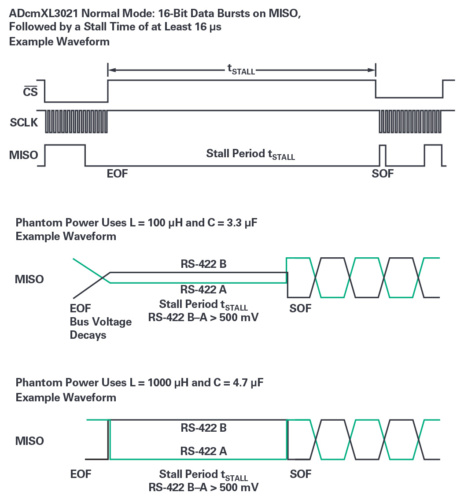
Figure 12. DC correctness on phantom power wires.
Wired Evaluation Solution
Analog Devices has developed the Pioneer 1 wired system evaluation solution to support the ADcmXL3021 triaxial MEMS accelerometer. The Pioneer 1 evaluation kits, as described in this wiki guide, can also support the MEMS devices shown in Table 5 with the help of the expansion board described in the wiki guide.
Table 5. Wired Evaluation Solution for MEMS Sensors
| Part | Noise Density | Range (g) | BW (Hz) | # Axes |
| ADcmXL3021 | 26 | 50 | 10000 | 3 |
| ADXL357 | 80 | 10, 20, 40 | 1000 | 3 |
| ADXL372 | 200 | 3200 | 3 |
| ADXL355 | 20 | 2, 4, 8 | 1000 | 3 |
| ADXL313 | 250 | 0.5, 1, 2, 4 | 1600 | 3 |
| ADXL363 | 550 | 2, 4, 8 | 200 | 3 |
| ADXL375 | 200 | 1600 | 3 |
| ADXL362 | 175 | 2, 4, 8 | 200 | 3 |
| ADXL345 | 420 | 2, 4, 8, 16 | 1600 | 3 |
| ADXL350 | 1, 2, 4, 8 | 1600 | 3 |
| ADXL343 | 2, 4, 8, 16 | 1600 | 3 |
| ADXL312 | 340 | 1.5, 3, 6, 12 | 1600 | 3 |
References
1 Richard Anslow and Dara O’Sullivan. “Enabling Robust Wired Condition-Based Monitoring for Industry 4.0—Part 1.” Analog Devices, Inc., July 2019.
2 “IEEE 802.3bu-2016—IEEE Standard for Ethernet—Amendment 8: Physical Layer and Management Parameters for Power over Data Lines(PoDL) of Single Balanced Twisted-Pair Ethernet.” IEEE, February 2017.
3 Andy Gardner. “PoDL: Decoupling Network Presentation.” Linear Technology, May 2014.
4 Andy Gardner. “Momentary PoDL Connector and Cable Shorts.” Linear Technology, September 2014.
About the Authors
Richard Anslow is a system applications engineer with the Connected Motion and Robotics Team within the Automation and Energy Business Unit at Analog Devices. His areas of expertise are condition-based monitoring and industrial communication design. He received his B.Eng. and M.Eng. degrees from the University of Limerick, Limerick, Ireland. He can be reached at richard.anslow@analog.com.
Dara O’Sullivan is a system applications manager with the Connected Motion and Robotics Team within the Automation and Energy Business Unit at Analog Devices. His area of expertise is power conversion, control, and monitoring in industrial motion control applications. He received his B.E., M.Eng.Sc., and Ph.D. from University College Cork, Ireland, and has worked in industrial and renewable energy applications in a range of research,consultancy, and industry positions since 2001. He can be reached at dara.osullivan@analog.com


UK Enters ‘Golden Age of Nuclear’
While I welcome the announcement of this project, I note that the original budget cost for Hinkley Point C was £18 billion and this has constantly...